SLLSFO5A November 2021 – September 2022 TRSF3243E
PRODUCTION DATA
- 1 Features
- 2 Applications
- 3 Description
- 4 Revision History
- 5 Pin Configuration and Functions
-
6 Specifications
- 6.1 Absolute Maximum Ratings
- 6.2 ESD Ratings
- 6.3 ESD Ratings - IEC Specifications
- 6.4 Recommended Operating Conditions
- 6.5 Thermal Information
- 6.6 Electrical Characteristics
- 6.7 Electrical Characteristics: Driver
- 6.8 Switching Characteristics: Driver
- 6.9 Electrical Characteristics: Receiver
- 6.10 Switching Characteristics: Receiver
- 6.11 Electrical Characteristics: Auto-Powerdown
- 6.12 Switching Characteristics: Auto-Powerdown
- 7 Detailed Description
- 8 Application and Implementation
- 9 Power Supply Recommendations
- 10Layout
- 11Mechanical, Packaging, and Orderable Information
Package Options
Mechanical Data (Package|Pins)
Thermal pad, mechanical data (Package|Pins)
Orderable Information
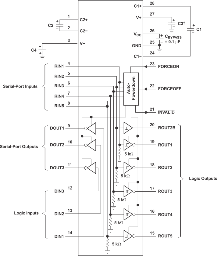
8.2 Typical Application
Three driver and five receiver channels are supported for full duplex transmission with hardware flow control. The five 5-kΩ resistors are internal to the device.

A. C3 can be connected to
VCC or GND
B. Resistor values shown are
nominal.
Figure 8-1 Typical
Operating Circuit and Capacitor Values