SCDS227F July 2006 – March 2015 TS3A4751
PRODUCTION DATA.
- 1 Features
- 2 Applications
- 3 Description
- 4 Revision History
- 5 Pin Configuration and Functions
- 6 Specifications
- 7 Detailed Description
- 8 Application and Implementation
- 9 Power Supply Recommendations
- 10Layout
- 11Device and Documentation Support
- 12Mechanical, Packaging, and Orderable Information
Package Options
Mechanical Data (Package|Pins)
Thermal pad, mechanical data (Package|Pins)
Orderable Information
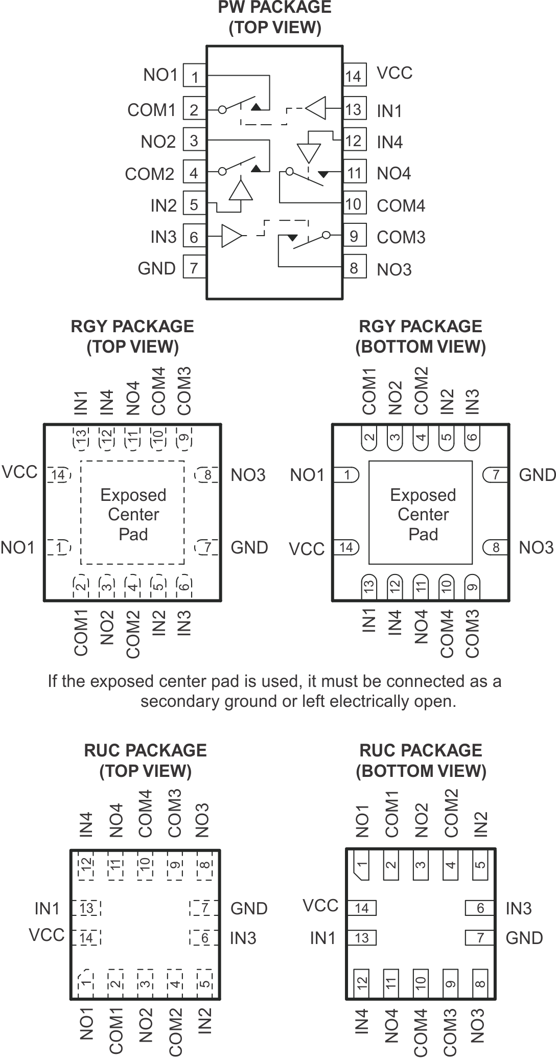
5 Pin Configuration and Functions

Pin Functions
| PIN | I/O | DESCRIPTION | |
|---|---|---|---|
| NO. | NAME | ||
| 1 | NO1 | I/O | Normally open signal path |
| 2 | COM1 | I/O | Common signal path |
| 3 | NO2 | I/O | Normally open signal path |
| 4 | COM2 | I/O | Common signal path |
| 5 | IN2 | I | Logic control input |
| 6 | IN3 | I | Logic control input |
| 7 | GND | — | Ground |
| 8 | NO3 | I/O | Normally open signal path |
| 9 | COM3 | I/O | Common signal path |
| 10 | COM4 | I/O | Common signal path |
| 11 | NO4 | I/O | Normally open signal path |
| 12 | IN4 | I | Logic control input |
| 13 | IN1 | I | Logic control input |
| 14 | VCC | I | Positive supply voltage |