SCDS430A December 2020 – May 2021 TS3DV642-Q1
PRODUCTION DATA
- 1 Features
- 2 Applications
- 3 Description
- 4 Revision History
- 5 Pin Configuration and Functions
- 6 Specifications
- 7 Parameter Measurement Information
- 8 Detailed Description
- 9 Application and Implementation
- 10Power Supply Recommendations
- 11Layout
- 12Device and Documentation Support
- 13Mechanical, Packaging, and Orderable Information
Package Options
Refer to the PDF data sheet for device specific package drawings
Mechanical Data (Package|Pins)
- RUA|42
Thermal pad, mechanical data (Package|Pins)
Orderable Information
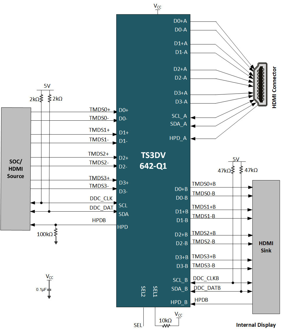
9.2 Typical Application - Demultiplexing HDMI Signals
The TS3DV642-Q1 can be used to mux HDMI signals. Figure 9-1 shows use case where TS3DV642-Q1 switches HDMI signals from a source to either to an external connector or to an SOC. This section provides detailed design implementation for a HDMI application where TS3DV642-Q1 provides 1:2 multiplexing function.
 Figure 9-1 Demultiplexing HDMI signals - schematic