SCDS348C September 2013 – March 2017 TS3USB3031
PRODUCTION DATA.
- 1 Features
- 2 Applications
- 3 Description
- 4 Revision History
- 5 Pin Configuration and Functions
- 6 Specifications
- 7 Parameter Measurement Information
- 8 Detailed Description
- 9 Application and Implementation
- 10Power Supply Recommendations
- 11Layout
- 12Device and Documentation Support
- 13Mechanical, Packaging, and Orderable Information
Package Options
Mechanical Data (Package|Pins)
- RMG|12
Thermal pad, mechanical data (Package|Pins)
Orderable Information
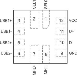
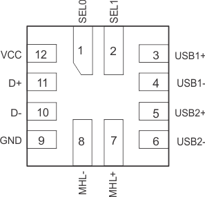
5 Pin Configuration and Functions
RMG Package
12-Pin VQFN
Top View

RMG Package
12-Pin VQFN
Bottom View

Pin Functions
| PIN | TYPE(1) | DESCRIPTION | |
|---|---|---|---|
| NO. | NAME | ||
| 1 | SEL0 | I | Digital control Input |
| 2 | SEL1 | I | Digital control Input |
| 3 | USB1+ | I/O | Differential signal path 1 |
| 4 | USB1– | I/O | Differential signal path 1 |
| 5 | USB2+ | I/O | Differential signal path 2 |
| 6 | USB2– | I/O | Differential signal path 2 |
| 7 | MHL+ | I/O | Differential signal path 3 |
| 8 | MHL– | I/O | Differential signal path 3 |
| 9 | GND | G | Ground |
| 10 | D– | I/O | Common Differential signal path |
| 11 | D+ | I/O | Common Differential signal path |
| 12 | VCC | P | Power Supply |
(1) G = Ground, I = Input, O = Output, P = Power