SCDS187C FEBRUARY 2005 – August 2018 TS5A3167
PRODUCTION DATA.
- 1 Features
- 2 Applications
- 3 Description
- 4 Revision History
- 5 Pin Configuration and Functions
-
6 Specifications
- 6.1 Absolute Maximum Ratings
- 6.2 ESD Ratings
- 6.3 Recommended Operating Conditions
- 6.4 Thermal Information
- 6.5 Electrical Characteristics for 5-V Supply
- 6.6 Electrical Characteristics for 5-V Supply (continued)
- 6.7 Electrical Characteristics for 3.3-V Supply
- 6.8 Electrical Characteristics for 3.3-V Supply (continued)
- 6.9 Electrical Characteristics for 2.5-V Supply
- 6.10 Electrical Characteristics for 2.5-V Supply (continued)
- 6.11 Electrical Characteristics for 1.8-V Supply
- 6.12 Electrical Characteristics for 1.8-V Supply (continued)
- 6.13 Typical Performance
- 7 Parameter Measurement Information
- 8 Detailed Description
- 9 Application and Implementation
- 10Power Supply Recommendations
- 11Layout
- 12Device and Documentation Support
- 13Mechanical, Packaging, and Orderable Information
Package Options
Refer to the PDF data sheet for device specific package drawings
Mechanical Data (Package|Pins)
- DBV|5
- DCK|5
- YZP|5
Thermal pad, mechanical data (Package|Pins)
Orderable Information
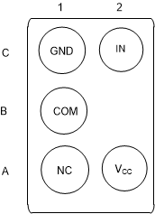
5 Pin Configuration and Functions
DBV or DCK Package
5- Pin (SOT-23 or SC70)
Top View

Pin Functions
| PIN NUMBER | NAME | DESCRIPTION |
|---|---|---|
| 1 | NC | Normally Closed |
| 2 | COM | Common |
| 3 | GND | Ground |
| 4 | IN | Digital control pin, COM connected to NC when logic low |
| 5 | VCC | Power Supply |
Pin Functions
| PIN NUMBER | NAME | DESCRIPTION |
|---|---|---|
| A1 | NC | Normally Closed |
| B1 | COM | Common |
| C1 | GND | Ground |
| A2 | VCC | Power Supply |
| C2 | IN | Digital control pin, COM connected to NC when logic low |
