SBOS878D July 2017 – October 2019 TSV911 , TSV912 , TSV914
PRODUCTION DATA.
- 1 Features
- 2 Applications
- 3 Description
- 4 Revision History
- 5 Device Comparison Table
- 6 Pin Configuration and Functions
- 7 Specifications
- 8 Detailed Description
- 9 Application and Implementation
- 10Power Supply Recommendations
- 11Layout
- 12Device and Documentation Support
- 13Mechanical, Packaging, and Orderable Information
Package Options
Refer to the PDF data sheet for device specific package drawings
Mechanical Data (Package|Pins)
- DBV|5
- DCK|5
Thermal pad, mechanical data (Package|Pins)
Orderable Information
6 Pin Configuration and Functions
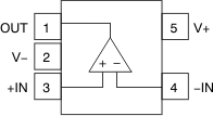
TSV911 DBV Package
5-Pin SOT-23
Top View

Pin Functions: TSV911
| PIN | I/O | DESCRIPTION | ||
|---|---|---|---|---|
| NAME | NO. | |||
| DBV (SOT-23) | DCK (SC70) | |||
| –IN | 4 | 3 | I | Inverting input |
| +IN | 3 | 1 | I | Noninverting input |
| OUT | 1 | 4 | O | Output |
| V– | 2 | 2 | — | Negative (lowest) supply or ground (for single-supply operation) |
| V+ | 5 | 5 | — | Positive (highest) supply |
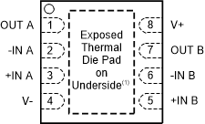
TSV912 DSG Package
8-Pin WSON With Exposed Thermal Pad
Top View

1. Connect exposed thermal pad to V–. See Packages with an Exposed Thermal Pad section for more information.
Pin Functions: TSV912
| PIN | I/O | DESCRIPTION | |
|---|---|---|---|
| NAME | NO. | ||
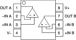
| –IN A | 2 | I | Inverting input, channel A |
| +IN A | 3 | I | Noninverting input, channel A |
| –IN B | 6 | I | Inverting input, channel B |
| +IN B | 5 | I | Noninverting input, channel B |
| OUT A | 1 | O | Output, channel A |
| OUT B | 7 | O | Output, channel B |
| V– | 4 | — | Negative (lowest) supply or ground (for single-supply operation) |
| V+ | 8 | — | Positive (highest) supply |
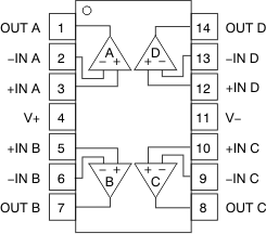
Pin Functions: TSV914
| PIN | I/O | DESCRIPTION | |
|---|---|---|---|
| NAME | NO. | ||
| –IN A | 2 | I | Inverting input, channel A |
| +IN A | 3 | I | Noninverting input, channel A |
| –IN B | 6 | I | Inverting input, channel B |
| +IN B | 5 | I | Noninverting input, channel B |
| –IN C | 9 | I | Inverting input, channel C |
| +IN C | 10 | I | Noninverting input, channel C |
| –IN D | 13 | I | Inverting input, channel D |
| +IN D | 12 | I | Noninverting input, channel D |
| OUT A | 1 | O | Output, channel A |
| OUT B | 7 | O | Output, channel B |
| OUT C | 8 | O | Output, channel C |
| OUT D | 14 | O | Output, channel D |
| V– | 11 | — | Negative (lowest) supply or ground (for single-supply operation) |
| V+ | 4 | — | Positive (highest) supply |

