SLLSEL4A September 2014 – October 2014 TUSB1210-Q1
PRODUCTION DATA.
- 1 Features
- 2 Applications
- 3 Description
- 4 Revision History
- 5 Pin Configuration and Functions
-
6 Specifications
- 6.1 Absolute Maximum Ratings
- 6.2 Handling Ratings
- 6.3 Recommended Operating Conditions
- 6.4 Thermal Information
- 6.5 Analog I/O Electrical Characteristics
- 6.6 Digital I/O Electrical Characteristics
- 6.7 Digital IO Pins (Non-ULPI)
- 6.8 PHY Electrical Characteristics
- 6.9 Pullup/Pulldown Resistors
- 6.10 OTG Electrical Characteristics
- 6.11 Power Characteristics
- 6.12 Switching Characteristics
- 6.13 Timing Requirements
- 6.14 Typical Characteristics
-
7 Detailed Description
- 7.1 Overview
- 7.2 Functional Block Diagram
- 7.3 Feature Description
- 7.4 Device Functional Modes
- 7.5
Register Map
- 7.5.1 VENDOR_ID_LO
- 7.5.2 VENDOR_ID_HI
- 7.5.3 PRODUCT_ID_LO
- 7.5.4 PRODUCT_ID_HI
- 7.5.5 FUNC_CTRL
- 7.5.6 FUNC_CTRL_SET
- 7.5.7 FUNC_CTRL_CLR
- 7.5.8 IFC_CTRL
- 7.5.9 IFC_CTRL_SET
- 7.5.10 IFC_CTRL_CLR
- 7.5.11 OTG_CTRL
- 7.5.12 OTG_CTRL_SET
- 7.5.13 OTG_CTRL_CLR
- 7.5.14 USB_INT_EN_RISE
- 7.5.15 USB_INT_EN_RISE_SET
- 7.5.16 USB_INT_EN_RISE_CLR
- 7.5.17 USB_INT_EN_FALL
- 7.5.18 USB_INT_EN_FALL_SET
- 7.5.19 USB_INT_EN_FALL_CLR
- 7.5.20 USB_INT_STS
- 7.5.21 USB_INT_LATCH
- 7.5.22 DEBUG
- 7.5.23 SCRATCH_REG
- 7.5.24 SCRATCH_REG_SET
- 7.5.25 SCRATCH_REG_CLR
- 7.5.26 VENDOR_SPECIFIC1
- 7.5.27 VENDOR_SPECIFIC1_SET
- 7.5.28 VENDOR_SPECIFIC1_CLR
- 7.5.29 VENDOR_SPECIFIC2
- 7.5.30 VENDOR_SPECIFIC2_SET
- 7.5.31 VENDOR_SPECIFIC2_CLR
- 7.5.32 VENDOR_SPECIFIC1_STS
- 7.5.33 VENDOR_SPECIFIC1_LATCH
- 7.5.34 VENDOR_SPECIFIC3
- 7.5.35 VENDOR_SPECIFIC3_SET
- 7.5.36 VENDOR_SPECIFIC3_CLR
- 8 Application and Implementation
- 9 Power Supply Recommendations
- 10Layout
- 11Device and Documentation Support
- 12Mechanical, Packaging, and Orderable Information
Package Options
Mechanical Data (Package|Pins)
- RHB|32
Thermal pad, mechanical data (Package|Pins)
- RHB|32
Orderable Information
1 Features
- AEC-Q100 Qualified with:
- Temperature Grade 3: –40°C to 85°C
- HBM ESD Classification 1C
- CDM ESD Classification C4B
- USB2.0 PHY Transceiver Chip, Designed to Interface with a USB Controller via a ULPI 12-pin Interface, Fully Compliant With:
- Universal Serial Bus Specification Rev. 2.0
- On-The-Go Supplement to the USB 2.0 Specification Rev. 1.3
- UTMI+ Low Pin Interface (ULPI) Specification Rev. 1.1
- DP/DM Line External Component Compensation (Patent #US7965100 B1)
- Interfaces to Host, Peripheral and OTG Device Cores; Optimized for Portable Devices or System ASICs with Built-in USB OTG Device Core
- Complete USB OTG Physical Front-End that Supports Host Negotiation Protocol (HNP) and Session Request Protocol (SRP)
- ULPI Interface:
- I/O Interface (1.8 V) Optimized for Non-Terminated 50 Ω Line Impedance
- ULPI CLOCK Pin (60 MHz) Supports Both Input and Output Clock Configurations
- Fully Programmable ULPI-Compliant Register Set
- Available in a 32-Pin Quad Flat No Lead
[QFN (RHB)] Package
2 Applications
- Mobile Phones
- Tablet Devices
- Desktop Computers
- Portable Computers
- Video Game Consoles
- Portable Music Players
3 Description
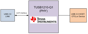
The TUSB1210-Q1 is a USB2.0 transceiver chip, designed to interface with a USB controller via a ULPI interface. It supports all USB2.0 data rates (High-Speed 480 Mbps, Full-Speed 12 Mbps and Low-Speed 1.5 Mbps), and is compliant to both Host and Peripheral modes. It additionally supports a UART mode and legacy ULPI serial modes.
TUSB1210-Q1 also supports the OTG (Ver1.3) optional addendum to the USB 2.0 Specification, including Host Negotiation Protocol (HNP) and Session Request Protocol (SRP).
The DP/DM external component compensation in the transmitter compensates for variations in the series impendence in order to match with the data line impedance and the receiver input impedance, to limit data reflections, and thereby, improve eye diagrams.
Device Information(1)
| PART NUMBER | PACKAGE | BODY SIZE (NOM) |
|---|---|---|
| TUSB1210-Q1 | VQFN (32) | 5.00 mm x 5.00 mm |
- For all available packages, see the orderable addendum at the end of the datasheet.
4 Revision History
Changes from * Revision (September 2014) to A Revision
- Changed the Features list Go
- Deleted 5 paragraphs from the Description following: "TUSB1210-Q1 also supports the OTG (Ver1.3).."Go
- Changed the Diagram imageGo
- Added VIL and VIH to the Recommended Operating Conditions table Go
- Changed the Thermal Information table Go
- Changed the Digital I/O Electrical Characteristics table Go
- Digital IO Electrical Characteristics sections to the Switching CharacteristicsGo
- Added the Typical Characteristics sectionGo
- Added 5 new paragraphs to the Overview sectionGo