SLLSFM9A March 2021 – December 2023 TUSB216I
PRODUCTION DATA
- 1
- 1 Features
- 2 Applications
- 3 Description
- 4 Device Comparison
- 5 Pin Configuration and Functions
- 6 Specifications
- 7 Detailed Description
- 8 Application and Implementation
- 9 Device and Documentation Support
- 10Revision History
- 11Mechanical, Packaging, and Orderable Information
Package Options
Refer to the PDF data sheet for device specific package drawings
Mechanical Data (Package|Pins)
- RWB|12
Thermal pad, mechanical data (Package|Pins)
Orderable Information
3 Description
The TUSB216I is a third-generation USB 2.0 high-speed signal conditioner designed to compensate both AC loss (due to capacitive load) and DC loss (due to resistive loss) in the transmission channel.
The TUSB216I leverages a patented design to speed-up transition edges of USB 2.0 high-speed signal with an edge booster and increases static levels with a DC boost function.
In addition, the TUSB216I includes a pre-equalization function to improve the receiver sensitivity and compensate the inter-symbol interference (ISI) jitter in application with longer cable length. USB low-speed and full-speed signal characteristics are unaffected by the TUSB216I.
The TUSB216I improves signal quality without altering packet timing or adding propagation delay or latency.
The TUSB216I helps a system to pass the USB 2.0 high-speed near end eye compliance with a cable as long as 5 meters.
The TUSB216I is compatible with the USB On-The-Go (OTG) and battery charging (BC 1.2) protocols. The Integrated BC 1.2 battery charging controller can be enabled through a control pin.
| PART NUMBER(1) | PACKAGE(2) | OP TEMP (TA) °C | PACKAGE SIZE(3) |
|---|---|---|---|
| TUSB216 | RWB (X2QFN, 12) | 0 to 70 | 1.6 mm × 1.6 mm |
| TUSB216I | -40 to 85 | ||
| TUSB216-Q1 | -40 to 105 |
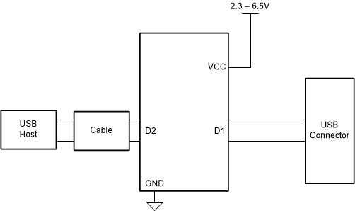
 Simplified Schematic