SLLSFK6 September 2021 TUSB217A-Q1
PRODUCTION DATA
- 1 Features
- 2 Applications
- 3 Description
- 4 Revision History
- 5 Device Comparison
- 6 Pin Configuration and Functions
- 7 Specifications
- 8 Detailed Description
- 9 Application and Implementation
- 10Power Supply Recommendations
- 11Layout
- 12Device and Documentation Support
- 13Mechanical, Packaging, and Orderable Information
Package Options
Mechanical Data (Package|Pins)
- RWB|12
Thermal pad, mechanical data (Package|Pins)
Orderable Information
6 Pin Configuration and Functions
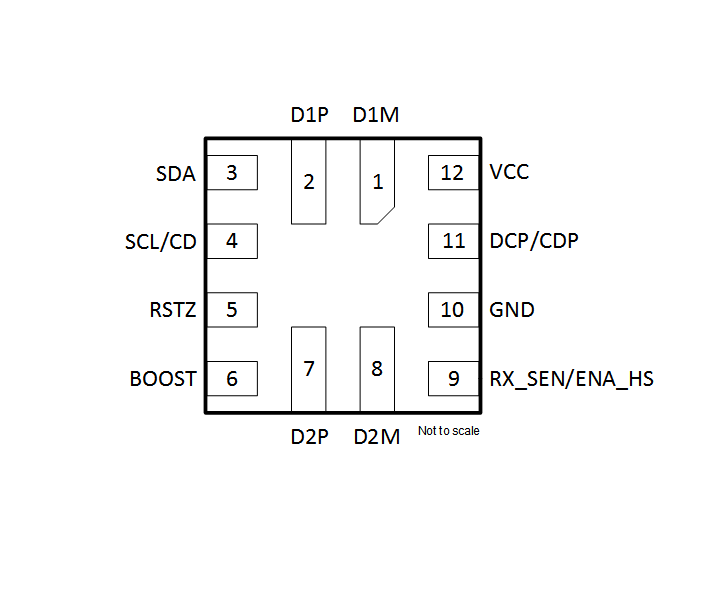
 Figure 6-1 TUSB217A-Q1
RWB12-Pin
X2QFNTop
View
Figure 6-1 TUSB217A-Q1
RWB12-Pin
X2QFNTop
ViewTable 6-1 Pin Functions
| PIN (RWB) | I/O | INTERNAL PULLUP/PULLDOWN |
DESCRIPTION | |
|---|---|---|---|---|
| NAME | NO. (RWB) | |||
| BOOST | 6 | I | N/A | USB High-speed boost select through the external pull down
resistor. Both edge boost and DC boost are controlled by a single pin in non-I2C mode. In I2C mode edge boost and DC boost can be individually controlled. Sampled upon power up. Does not recognize real time adjustments. Auto selects BOOST LEVEL = 3 when left floating. |
| DCP/CDP | 11 | I | 500 kΩ PU | DCP or CDP mode selection. Low=DCP and High=CDP TUSB217A-Q1RWB BC1.2 controller is always enabled. |
| RX_SEN(2)/ENA_HS | 9 | I/O | N/A | In I2C mode: Reserved for TI test purpose. In non-I2C mode: At reset: 3-level input signal RX_SEN. USB High-speed RX Equalization Setting to Compensate ISI Jitter H (pin is pulled high) – high RX equalization (high loss channel) M (pin is left floating) – medium RX equalization (medium loss channel) L (pin is pulled low) – low RX equalization (low loss channel) After reset: Output signal ENA_HS. Flag indicating that channel is in High-speed mode. Asserted upon: 1. Detection of USB-IF High-speed test fixture from an unconnected state followed by transmission of USB TEST_PACKET pattern. 2. Squelch detection following USB reset with a successful HS handshake [HS handshake is declared to be successful after single chirp J chirp K pair where each chirp is within 18 μs – 128 μs]. |
| D2P | 7 | I/O | N/A | USB High-speed positive port. |
| D2M | 8 | I/O | N/A | USB High-speed negative port. |
| GND | 10 | P | N/A | Ground |
| D1M | 1 | I/O | N/A | USB High-speed negative port.. |
| D1P | 2 | I/O | N/A | USB High-speed positive port. |
| SDA(1) | 3 | I/O | 500 kΩ PU 1.8 MΩ PD |
I2C Mode: Bidirectional I2C data pin [7-bit I2C slave address = 0x2C]. In non I2C mode: Reserved for TI test purpose. |
| VCC | 12 | P | N/A | Supply power |
| RSTN | 5 | I | 500 kΩ PU 1.8 MΩ PD |
Device
disable/enable. Low – Device is at reset and in shutdown, and High - Normal operation. Recommend 0.1-µF external capacitor to GND to ensure clean power on reset if not driven. If the pin is driven, it must be held low until the supply voltage for the device reaches within specifications. |
| SCL(1)/CD | 4 | I/O | When RSTN asserted there is a 500 kΩ PD | In I2C mode: I2C clock pin [I2C address = 0x2C]. Non I2C mode: After reset: Output CD. Flag indicating that a USB device is attached (connection detected). Asserted from an unconnected state upon detection of DP or DM pull-up resistor. De-asserted upon detection of disconnect. |
(1) Pull-up resistors for SDA and SCL pins in I2C mode should be
RPull-up (depending on I2C bus voltage). If both SDA and SCL are pulled up at
power-up the device enters into I2C mode.
(2) Pull-down and pull-up resistors for RX_SEN pin must follow
RRXSEN1 and RRXSEN2 resistor recommendations in non I2C
mode.