SCES650J April 2006 – October 2020 TXB0104
PRODUCTION DATA
- 1 Features
- 2 Applications
- 3 Description
- 4 Revision History
- 5 Pin Configuration and Functions
-
6 Specifications
- 6.1 Absolute Maximum Ratings
- 6.2 ESD Ratings
- 6.3 Recommended Operating Conditions
- 6.4 Thermal Information
- 6.5 Electrical Characteristics
- 6.6 Timing Requirements: VCCA = 1.2 V
- 6.7 Timing Requirements: VCCA = 1.5 V ± 0.1 V
- 6.8 Timing Requirements: VCCA = 1.8 V ± 0.15 V
- 6.9 Timing Requirements: VCCA = 2.5 V ± 0.2 V
- 6.10 Timing Requirements: VCCA = 3.3 V ± 0.3 V
- 6.11 Switching Characteristics: VCCA = 1.2 V
- 6.12 Switching Characteristics: VCCA = 1.5 V ± 0.1 V
- 6.13 Switching Characteristics: VCCA = 1.8 V ± 0.15 V
- 6.14 Switching Characteristics: VCCA = 2.5 V ± 0.2 V
- 6.15 Switching Characteristics: VCCA = 3.3 V ± 0.3 V
- 6.16 Operating Characteristics: VCCA = 1.2 V to 1.5 V, VCCB = 1.5 V to 1.8 V
- 6.17 Operating Characteristics: VCCA = 1.8 V to 3.3 V, VCCB = 1.8 V to 5 V
- 6.18 Typical Characteristics
- 7 Parameter Measurement Information
- 8 Detailed Description
- 9 Application and Implementation
- 10Power Supply Recommendations
- 11Layout
- 12Device and Documentation Support
- 13Mechanical, Packaging, and Orderable Information
Package Options
Refer to the PDF data sheet for device specific package drawings
Mechanical Data (Package|Pins)
- D|14
- RGY|14
- RUT|12
- NMN|12
- YZT|12
- PW|14
Thermal pad, mechanical data (Package|Pins)
Orderable Information
3 Description
This TXB0104 4-bit noninverting translator uses two separate configurable power-supply rails. The A port is designed to track VCCA. VCCA accepts any supply voltage from 1.2 V to 3.6 V. The B port is designed to track VCCB. VCCB accepts any supply voltage from 1.65 V to 5.5 V. This allows for universal low-voltage bidirectional translation between any of the 1.2-V, 1.5-V, 1.8-V, 2.5-V, 3.3-V, and 5-V voltage nodes. VCCA must not exceed VCCB.
When the OE input is low, all outputs are placed in the high-impedance state. To ensure the high-impedance state during power up or power down, OE must be tied to GND through a pulldown resistor The current sourcing capability of the driver determines the minimum value of the resistor.
The TXB0104 device is designed so the OE input circuit is supplied by VCCA.
This device is fully specified for partial power-down applications using I OFF. The I OFF circuitry disables the outputs, which prevents damaging current backflow through the device when the device is powered down.
| (1)PART NUMBER | PACKAGE | BODY SIZE (NOM) |
|---|---|---|
| TXB0104RUT | UQFN (12) | 2.00 mm × 1.70 mm |
| TXB0104D | SOIC (14) | 8.65 mm × 3.91 mm |
| TXB0104ZXU/GXU | BGA MICROSTAR JUNIOR™ (12) | 2.00 mm × 2.50 mm |
| TXB0104PW | TSSOP (14) | 5.00 mm × 4.40 mm |
| TXB0104RGY | VQFN (14) | 3.50 mm × 3.50 mm |
| TXB0104YZT | DSBGA (12) | 1.40 mm × 1.90 mm |
| TXB0104NMN | NFBGA (12) | 2.00 mm × 2.50 mm |
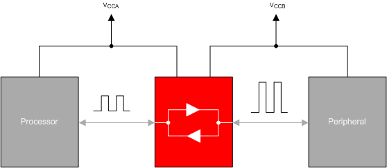
 Typical Application Block Diagram for TXB010X