SCES854A May 2014 – September 2017 TXS0102-Q1
PRODUCTION DATA.
- 1 Features
- 2 Applications
- 3 Description
- 4 Revision History
- 5 Pin Configuration and Functions
-
6 Specifications
- 6.1 Absolute Maximum Ratings
- 6.2 ESD Ratings
- 6.3 Recommended Operating Conditions
- 6.4 Thermal Information
- 6.5 Electrical Characteristics
- 6.6 Timing Requirements — VCCA = 1.8 V ± 0.15 V
- 6.7 Timing Requirements — VCCA = 2.5 V ± 0.2 V
- 6.8 Timing Requirements — VCCA = 3.3 V ± 0.3 V
- 6.9 Switching Characteristics — VCCA = 1.8 V ± 0.15 V
- 6.10 Switching Characteristics — VCCA = 2.5 V ± 0.2 V
- 6.11 Switching Characteristics — VCCA = 3.3 V ± 0.3 V
- 6.12 Typical Characteristics
- 7 Parameter Measurement Information
- 8 Detailed Description
- 9 Application and Implementation
- 10Power Supply Recommendations
- 11Layout
- 12Device and Documentation Support
- 13Mechanical, Packaging, and Orderable Information
Package Options
Mechanical Data (Package|Pins)
- DCU|8
Thermal pad, mechanical data (Package|Pins)
Orderable Information
7 Parameter Measurement Information
7.1 Load Circuits
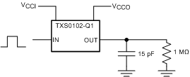 Figure 4. Data Rate, Pulse Duration, Propagation Delay, Output Rise-Time and Fall-Time Measurement Using a Push-Pull Driver
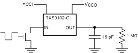 Figure 5. Data Rate, Pulse Duration, Propagation Delay, Output Rise-Time and Fall-Time Measurement Using an Open-Drain Driver
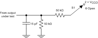
| TEST | S1 | ||
| tPZL / tPLZ
(tdis) |
2 × VCCO | ||
| tPHZ / tPZH
(ten) |
Open | ||
- tPLZ and tPHZ are the same as tdis.
- tPZL and tPZH are the same as ten.
- VCCI is the VCC associated with the input port.
- VCCO is the VCC associated with the output port.
7.2 Voltage Waveforms
 Figure 7. Pulse Duration
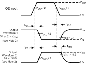 Figure 9. Enable and Disable Times
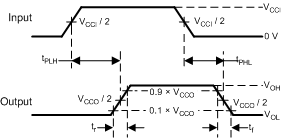 Figure 8. Propagation Delay Times
- CL includes probe and jig capacitance.
- Waveform 1 in Figure 9 is for an output with internal such that the output is high, except when OE is high (see Figure 6). Waveform 2 in Figure 9 is for an output with conditions such that the output is low, except when OE is high.
- All input pulses are supplied by generators having the following characteristics: PRR ≤ 10 MHz, ZO = 50 Ω, dv/dt ≥ 1 V/ns.
- The outputs are measured one at a time, with one transition per measurement.
- tPLZ and tPHZ are the same as tdis.
- tPZL and tPZH are the same as ten.
- tPLH and tPHL are the same as tpd.
- VCCI is the VCC associated with the input port.
- VCCO is the VCC associated with the output port.