SCES947 August 2022 TXU0101-Q1
PRODMIX
- 1 Features
- 2 Applications
- 3 Description
- 4 Revision History
- 5 Pin Configuration and Functions—TXU0101-Q1
-
6 Specifications
- 6.1 Absolute Maximum Ratings
- 6.2 ESD Ratings
- 6.3 Recommended Operating Conditions
- 6.4 Thermal Information
- 6.5 Electrical Characteristics
- 6.6 Switching Characteristics, VCCA = 1.2 ± 0.1 V
- 6.7 Switching Characteristics, VCCA = 1.5 ± 0.1 V
- 6.8 Switching Characteristics, VCCA = 1.8 ± 0.15 V
- 6.9 Switching Characteristics, VCCA = 2.5 ± 0.2 V
- 6.10 Switching Characteristics, VCCA = 3.3 ± 0.3 V
- 6.11 Switching Characteristics, VCCA = 5.0 ± 0.5 V
- 6.12 Operating Characteristics
- 6.13 Typical Characteristics
- 7 Parameter Measurement Information
-
8 Detailed Description
- 8.1 Overview
- 8.2 Functional Block Diagram
- 8.3
Feature Description
- 8.3.1 CMOS Schmitt-Trigger Inputs with Integrated Pulldowns
- 8.3.2 Control Logic (OE) with VCC(MIN) Circuitry
- 8.3.3 Balanced High-Drive CMOS Push-Pull Outputs
- 8.3.4 VCC Isolation and VCC Disconnect
- 8.3.5 Over-Voltage Tolerant Inputs
- 8.3.6 Glitch-Free Power Supply Sequencing
- 8.3.7 Negative Clamping Diodes
- 8.3.8 Fully Configurable Dual-Rail Design
- 8.3.9 Supports High-Speed Translation
- 8.4 Device Functional Modes
- 9 Application and Implementation
- 10Power Supply Recommendations
- 11Layout
- 12Device and Documentation Support
- 13Mechanical, Packaging, and Orderable Information
Package Options
Mechanical Data (Package|Pins)
Thermal pad, mechanical data (Package|Pins)
Orderable Information
8.3.4 VCC Isolation and VCC Disconnect
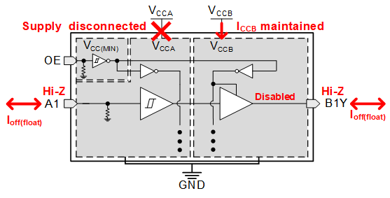
The outputs for this device disable and enter a high-impedance state when either supply is <100 mV or left floating (disconnected), with the complementary supply within the recommended operating conditions. It is recommended to keep the inputs low before floating (disconnecting) either supply.
The ICCx(floating) in the Electrical Characteristics specifies the maximum supply current. The Ioff(float) in the Electrical Characteristics specifies the maximum leakage into or out of any input or output pin on the device.
 Figure 8-1 VCC Disconnect
Feature