SCES941A November 2021 – March 2022 TXU0102
PRODUCTION DATA
- 1 Features
- 2 Applications
- 3 Description
- 4 Revision History
- 5 Related Products
- 6 Pin Configuration and Functions—TXU0102
-
7 Specifications
- 7.1 Absolute Maximum Ratings
- 7.2 ESD Ratings
- 7.3 Recommended Operating Conditions
- 7.4 Thermal Information
- 7.5 Electrical Characteristics
- 7.6 Switching Characteristics, VCCA = 1.2 ± 0.1 V
- 7.7 Switching Characteristics, VCCA = 1.5 ± 0.1 V
- 7.8 Switching Characteristics, VCCA = 1.8 ± 0.15 V
- 7.9 Switching Characteristics, VCCA = 2.5 ± 0.2 V
- 7.10 Switching Characteristics, VCCA = 3.3 ± 0.3 V
- 7.11 Switching Characteristics, VCCA = 5.0 ± 0.5 V
- 7.12 Operating Characteristics
- 7.13 Typical Characteristics
- 8 Parameter Measurement Information
-
9 Detailed Description
- 9.1 Overview
- 9.2 Functional Block Diagram
- 9.3
Feature Description
- 9.3.1 CMOS Schmitt-Trigger Inputs with Integrated Pulldowns
- 9.3.2 Control Logic (OE) with VCC(MIN) Circuitry
- 9.3.3 Balanced High-Drive CMOS Push-Pull Outputs
- 9.3.4 VCC Isolation and VCC Disconnect
- 9.3.5 Over-Voltage Tolerant Inputs
- 9.3.6 Glitch-Free Power Supply Sequencing
- 9.3.7 Negative Clamping Diodes
- 9.3.8 Fully Configurable Dual-Rail Design
- 9.3.9 Supports High-Speed Translation
- 9.4 Device Functional Modes
- 10Application and Implementation
- 11Power Supply Recommendations
- 12Layout
- 13Device and Documentation Support
- 14Mechanical, Packaging, and Orderable Information
Package Options
Mechanical Data (Package|Pins)
Thermal pad, mechanical data (Package|Pins)
Orderable Information
3 Description
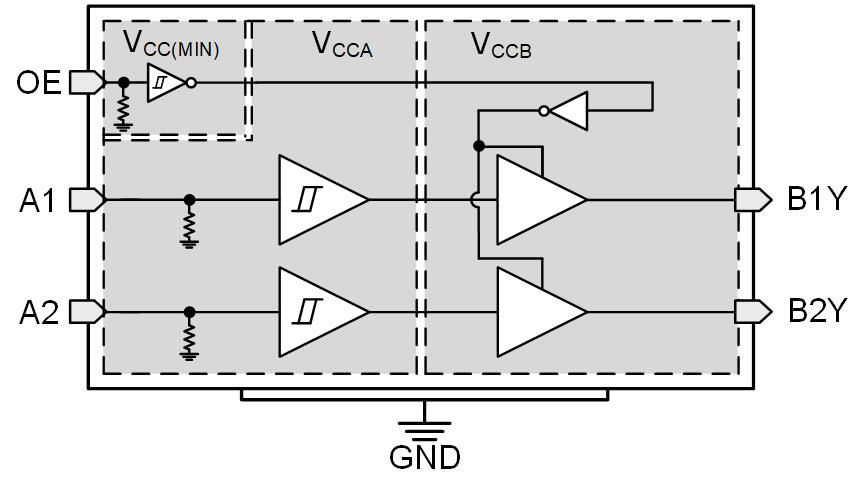
TXU0102 is a 2-bit, dual-supply noninverting fixed direction voltage level translation device. Ax pins are referenced to VCCA logic level, OE pin can be referenced to either VCCA or VCCB logic levels, and Bx pins are referenced to VCCB logic levels. The A port is able to accept input voltages ranging from 1.1 V to 5.5 V, while the B port can also accept input voltages from 1.1 V to 5.5 V. Fixed direction data transmission can occur from A to B or B to A when OE is set to high in reference to either supply. When OE is set to low, all output pins are in the high-impedance state. See Device Functional Modes for a summary of the operation of the control logic.
| DEVICE NUMBER | PACKAGE | BODY SIZE (NOM) |
|---|---|---|
| TXU0102 | VSSOP (DCU) (8) | 2.30 mm × 2.00 mm |
| SON (DTT) (8) | 1.95 mm × 1.00 mm | |
| X2SON (DTM) (8) | 1.35 mm × 0.80 mm |
 TXU0102 Functional Block Diagram