SLUSDD4B April 2019 – December 2020 UC1843B-SP
PRODUCTION DATA
- 1 Features
- 2 Applications
- 3 Description
- 4 Revision History
- 5 Pin Configuration and Functions
- 6 Specifications
- 7 Detailed Description
- 8 Application Information Disclaimer
- 9 Power Supply Recommendations
- 10Layout
- 11Device and Documentation Support
- 12Mechanical, Packaging, and Orderable Information
Package Options
Mechanical Data (Package|Pins)
- KGD|0
- HKU|10
Thermal pad, mechanical data (Package|Pins)
Orderable Information
7.3 Feature Description
UC1843B-SP is a current mode controller, used to support various topologies such as forward, flyback, buck, and boost. Using an external interface circuit will also support half-bridge, full-bridge, and push-pull configurations.
Figure 7-1 shows the two-loop current-mode control system. A clock signal initiates power pulses at a fixed frequency. The termination of each pulse occurs when an analog of the inductor current reaches a threshold established by the error signal. In this way, the error signal actually controls peak inductor current. This contrasts with voltage control in which the error signal directly controls pulse width without regard to inductor current.
Several performance advantages result from the use of current-mode control. First, an input voltage feed-forward characteristic is achieved; that is, the control circuit instantaneously corrects for input voltage variations without using up any of the error amplifier’s dynamic range. Therefore, line regulation is excellent and the error amplifier can be dedicated to correcting for load variations exclusively.
 Figure 7-1 Two-Loop Current-Mode Control System
For converters in which inductor current is continuous, controlling peak current is nearly equivalent to controlling average current. Therefore, when such converters employ current-mode control, the purposes of small signal analysis (see Figure 7-2). The two pole control to output frequency response of these converters is reduced to a single-pole (filter capacitor in parallel with load) response. One result is that the error amplifier compensation can be designed to yield a stable closed-loop converter response with greater gain bandwidth than would be possible with pulse-width control, giving the supply improved small signal dynamic response to changing loads. A second result is that the error amplifier compensation circuit becomes simpler, as shown in Figure 7-3.
Capacitor Ci and resistor Ri, in Figure 7-3(A), add a low frequency zero, which cancels one of the two control to output poles of non-current mode converters. For large signal load changes, in which converter response is limited by inductor slew rate, the error amplifier saturates while the inductor is catching up with the load. During this time, Ci charges to an abnormal level. When the inductor current reaches its required level, the voltage on Ci causes a corresponding error in supply output voltage. The recovery time is RizCi, which may be long. However, the compensation network of Figure 7-3(B) can be used where current-mode control has eliminated the inductor pole. Large-signal dynamic response is then greatly improved due to the absence of Ci.
Current limiting is greatly simplified with current mode control. Pulse-by-pulse limiting is, of course, inherent in the control scheme. Furthermore, an upper limit on the peak current can be established by simply clamping the error voltage. Accurate current limiting allows optimization of magnetic and power semiconductor elements while ensuring reliable supply operation.
Finally, current-mode controlled power stages can be operated in parallel with equal current sharing. This opens the possibility of a modular approach to power supply design.
 Figure 7-2 Inductor Looks Like a Current Source to Small Signals
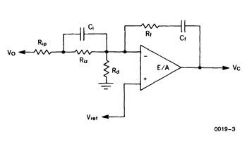 A. Direct duty cycle control | 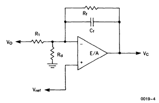 B. Current mode control |