SLUS557G March 2003 – December 2016 UC28023 , UC28025
PRODUCTION DATA.
- 1 Features
- 2 Applications
- 3 Description
- 4 Revision History
- 5 Pin Configuration and Functions
- 6 Specifications
- 7 Parameter Measurement Information
- 8 Detailed Description
- 9 Application and Implementation
- 10Power Supply Recommendations
- 11Layout
- 12Device and Documentation Support
- 13Mechanical, Packaging, and Orderable Information
Package Options
Refer to the PDF data sheet for device specific package drawings
Mechanical Data (Package|Pins)
- DW|16
- N|16
Thermal pad, mechanical data (Package|Pins)
Orderable Information
1 Features
- Peak Current Mode, Average Current Mode, or Voltage Mode (With FeedForward) Control Methods
- Practical Operation Up to 1 MHz
- 50-ns Propagation Delay to Output
- ±1.5-A Peak Totem Pole Outputs
- 9-V to 30-V Nominal Operational Voltage
- Wide Bandwidth Error Amplifier
- Fully Latched Logic With Double Pulse Suppression
- Pulse-by-Pulse Current Limiting
- Programmable Maximum Duty Cycle Control
- Undervoltage Lockout With Hysteresis
- Trimmed 5.1-V Reference With UVLO
- Same Functionality as UC3823 and UC3825
2 Applications
- Off-Line and DC-DC Power Supplies
- Converters Using Voltage Mode, Peak Current Mode, or Average Current Mode Control Methods
- Single-Ended or Two-Switch Topology Designs
3 Description
The UC28023 and UC28025 are fixed-frequency PWM controllers optimized for high-frequency switched-mode power-supply applications. The UC28023 is a single output PWM for single-ended topologies while the UC28025 offers dual alternating outputs for double-ended and full bridge topologies.
Targeted for cost-effective solutions with minimal external components. UC2802x devices include an oscillator, a temperature compensated reference, a wide bandwidth error amplifier, a high-speed current-sense comparator, and high-current, active-high, totem-pole outputs to directly drive external MOSFETs.
Protection circuitry includes a current limit comparator with a 1-V threshold, a TTL compatible shutdown port, and a soft-start pin which doubles as a maximum duty-cycle clamp. The logic is fully latched to provide jitter-free operation and prohibit multiple pulses at an output. An undervoltage lockout section with 800 mV of hysteresis assures low start-up current. During undervoltage lockout, the outputs are high impedance. Propagation delays through the comparators and logic circuitry have been minimized while maximizing bandwidth and slew rate of the error amplifier.
Devices are available in the industrial temperature range of –40°C to 105°C. Package offerings are
16-pin SOIC (DW), or 16-pin PDIP (N) packages.
Device Information(1)
| PART NUMBER | PACKAGE | BODY SIZE (NOM) |
|---|---|---|
| UC2802x | SOIC (16) | 10.30 mm × 7.50 mm |
| PDIP (16) | 19.30 mm × 6.35 mm |
- For all available packages, see the orderable addendum at the end of the data sheet.
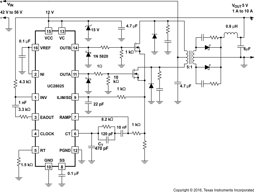
Typical Application Schematic
