SLUS223G April 1997 – July 2022 UC1842 , UC1843 , UC1844 , UC1845 , UC2842 , UC2843 , UC2844 , UC2845 , UC3842 , UC3843 , UC3844 , UC3845
PRODUCTION DATA
- 1 Features
- 2 Applications
- 3 Description
- 4 Revision History
- 5 Device Comparison Table
- 6 Pin Configuration and Functions
- 7 Specifications
-
8 Detailed Description
- 8.1 Overview
- 8.2 Functional Block Diagrams
- 8.3 Feature Description
- 8.4 Device Functional Modes
-
9 Application and Implementation
- 9.1 Application Information
- 9.2
Typical Application
- 9.2.1 Design Requirements
- 9.2.2
Detailed Design Procedure
- 9.2.2.1 Input Bulk Capacitor and Minimum Bulk Voltage
- 9.2.2.2 Transformer Turns Ratio and Maximum Duty Cycle
- 9.2.2.3 Transformer Inductance and Peak Currents
- 9.2.2.4 Output Capacitor
- 9.2.2.5 Current Sensing Network
- 9.2.2.6 Gate Drive Resistor
- 9.2.2.7 VREF Capacitor
- 9.2.2.8 RT/CT
- 9.2.2.9 Start-Up Circuit
- 9.2.2.10 Voltage Feedback Compensation
- 9.2.3 Application Curves
- 10Power Supply Recommendations
- 11Layout
- 12Device and Documentation Support
- 13Mechanical, Packaging, and Orderable Information
Package Options
Mechanical Data (Package|Pins)
Thermal pad, mechanical data (Package|Pins)
Orderable Information
8.3.5 Undervoltage Lockout
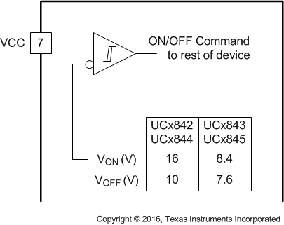
The UCx84x devices feature undervoltage lockout protection circuits for controlled operation during power-up and power-down sequences. The UVLO circuit insures that VCC is adequate to make the UCx84x fully operational before enabling the output stage. Undervoltage lockout thresholds for the UCx842, UCx843, UCx844, and UCx845 devices are optimized for two groups of applications: off-line power supplies and DC-DC converters. The 6-V hysteresis in the UCx842 and UCx844 devices prevents VCC oscillations during power sequencing. This wider VCCON to VCCOFF range, make these devices ideally suited to off-line AC input applications. The UCx843 and UCx845 controllers have a much narrower VCCON to VCCOFF hysteresis and may be used in DC to DC applications where the input is considered regulated.
Start-up current is less than 1 mA for efficient bootstrapping from the rectified input of an off-line converter, as illustrated by Figure 8-7. During normal circuit operation, VCC is developed from auxiliary winding NA with DBIAS and CVCC. At start-up, however, CVCC must be charged to 16 V through RSTART. With a start-up current of 1 mA, RSTART can be as large as 100 kΩ and still charge CVCC when VAC = 90 V RMS (low line). Power dissipation in RSTART would then be less than 350 mW even under high line (VAC= 130 V RMS) conditions.
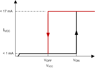
During UVLO the IC draws less than 1 mA of supply current. Once crossing the turnon threshold the IC supply current increases to a maximum of 17 mA, typically 11 mA, During undervoltage lockout, the output driver is biased to a high impedance state and sinks minor amounts of current. A bleeder resistor, placed between the gate and the source of the MOSFET should be used to prevent activating the power switch with extraneous leakage currents during undervoltage lockout.
 Figure 8-5 UVLO Threshold
 Figure 8-6 UVLO ON and OFF Profile
 Figure 8-7 Providing Power to UCx84x