SLUS223G April 1997 – July 2022 UC1842 , UC1843 , UC1844 , UC1845 , UC2842 , UC2843 , UC2844 , UC2845 , UC3842 , UC3843 , UC3844 , UC3845
PRODUCTION DATA
- 1 Features
- 2 Applications
- 3 Description
- 4 Revision History
- 5 Device Comparison Table
- 6 Pin Configuration and Functions
- 7 Specifications
-
8 Detailed Description
- 8.1 Overview
- 8.2 Functional Block Diagrams
- 8.3 Feature Description
- 8.4 Device Functional Modes
-
9 Application and Implementation
- 9.1 Application Information
- 9.2
Typical Application
- 9.2.1 Design Requirements
- 9.2.2
Detailed Design Procedure
- 9.2.2.1 Input Bulk Capacitor and Minimum Bulk Voltage
- 9.2.2.2 Transformer Turns Ratio and Maximum Duty Cycle
- 9.2.2.3 Transformer Inductance and Peak Currents
- 9.2.2.4 Output Capacitor
- 9.2.2.5 Current Sensing Network
- 9.2.2.6 Gate Drive Resistor
- 9.2.2.7 VREF Capacitor
- 9.2.2.8 RT/CT
- 9.2.2.9 Start-Up Circuit
- 9.2.2.10 Voltage Feedback Compensation
- 9.2.3 Application Curves
- 10Power Supply Recommendations
- 11Layout
- 12Device and Documentation Support
- 13Mechanical, Packaging, and Orderable Information
Package Options
Mechanical Data (Package|Pins)
Thermal pad, mechanical data (Package|Pins)
Orderable Information
3 Description
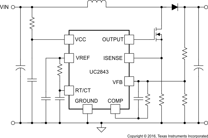
The UCx84x series of control integrated circuits provide the features that are necessary to implement off-line or DC-to-DC fixed-frequency current-mode control schemes, with a minimum number of external components. The internally implemented circuits include an undervoltage lockout (UVLO), featuring a start-up current of less than 1 mA, and a precision reference trimmed for accuracy at the error amplifier input. Other internal circuits include logic to ensure latched operation, a pulse-width modulation (PWM) comparator that also provides current-limit control, and a totem-pole output stage that is designed to source or sink high-peak current. The output stage, suitable for driving N-channel MOSFETs, is low when it is in the off state.
The UCx84x family offers a variety of package options, temperature range options, choice of maximum duty cycle, and choice of turnon and turnoff thresholds and hysteresis ranges. Devices with higher turnon or turnoff hysteresis are ideal choices for off-line power supplies, while the devices with a narrower hysteresis range are suited for DC-DC applications. The UC184x devices are specified for operation from –55°C to 125°C, the UC284x series is specified for operation from –40°C to 85°C, and the UC384x series is specified for operation from 0°C to 70°C.
| PART NUMBER | PACKAGE (PIN) | BODY SIZE (NOM) |
|---|---|---|
| UC184x | CDIP (8) | 9.60 mm × 6.67 mm |
| LCCC (20) | 8.89 mm × 8.89 mm | |
| CFP (8) | 9.21 mm × 5.97 mm | |
| UC284x | SOIC (8) | 4.90 mm × 3.91 mm |
| SOIC (14) | 8.65 mm × 3.91 mm | |
| PDIP (8) | 9.81 mm × 6.35 mm | |
| UC384x | SOIC (8) | 4.90 mm × 3.91 mm |
| SOIC (14) | 8.65 mm × 3.91 mm | |
| PDIP (8) | 9.81 mm × 6.35 mm | |
| CFP (8) | 9.21 mm × 5.97 mm |
 Simplified Application