SLUSCQ2D October   2017  – June 2020 UCC21520-Q1

PRODUCTION DATA.  

  1. Features
  2. Applications
  3. Description
    1.     Functional Block Diagram
  4. Revision History
  5. Pin Configuration and Functions
    1.     Pin Functions
  6. Specifications
    1. 6.1  Absolute Maximum Ratings
    2. 6.2  ESD Ratings
    3. 6.3  Recommended Operating Conditions
    4. 6.4  Thermal Information
    5. 6.5  Power Ratings
    6. 6.6  Insulation Specifications
    7. 6.7  Safety-Related Certifications
    8. 6.8  Safety-Limiting Values
    9. 6.9  Electrical Characteristics
    10. 6.10 Switching Characteristics
    11. 6.11 Insulation Characteristics Curves
    12. 6.12 Typical Characteristics
  7. Parameter Measurement Information
    1. 7.1 Propagation Delay and Pulse Width Distortion
    2. 7.2 Rising and Falling Time
    3. 7.3 Input and Disable Response Time
    4. 7.4 Programable Dead Time
    5. 7.5 Power-up UVLO Delay to OUTPUT
    6. 7.6 CMTI Testing
  8. Detailed Description
    1. 8.1 Overview
    2. 8.2 Functional Block Diagram
    3. 8.3 Feature Description
      1. 8.3.1 VDD, VCCI, and Under Voltage Lock Out (UVLO)
      2. 8.3.2 Input and Output Logic Table
      3. 8.3.3 Input Stage
      4. 8.3.4 Output Stage
      5. 8.3.5 Diode Structure in the UCC21520-Q1
    4. 8.4 Device Functional Modes
      1. 8.4.1 Disable Pin
      2. 8.4.2 Programmable Dead Time (DT) Pin
        1. 8.4.2.1 Tying the DT Pin to VCC
        2. 8.4.2.2 DT Pin Connected to a Programming Resistor between DT and GND Pins
  9. Application and Implementation
    1. 9.1 Application Information
    2. 9.2 Typical Application
      1. 9.2.1 Design Requirements
      2. 9.2.2 Detailed Design Procedure
        1. 9.2.2.1 Designing INA/INB Input Filter
        2. 9.2.2.2 Select External Bootstrap Diode and its Series Resistor
        3. 9.2.2.3 Gate Driver Output Resistor
        4. 9.2.2.4 Gate to Source Resistor Selection
        5. 9.2.2.5 Estimate Gate Driver Power Loss
        6. 9.2.2.6 Estimating Junction Temperature
        7. 9.2.2.7 Selecting VCCI, VDDA/B Capacitor
          1. 9.2.2.7.1 Selecting a VCCI Capacitor
          2. 9.2.2.7.2 Selecting a VDDA (Bootstrap) Capacitor
          3. 9.2.2.7.3 Select a VDDB Capacitor
        8. 9.2.2.8 Dead Time Setting Guidelines
        9. 9.2.2.9 Application Circuits with Output Stage Negative Bias
      3. 9.2.3 Application Curves
  10. 10Power Supply Recommendations
  11. 11Layout
    1. 11.1 Layout Guidelines
    2. 11.2 Layout Example
  12. 12Device and Documentation Support
    1. 12.1 Documentation Support
      1. 12.1.1 Related Documentation
    2. 12.2 Certifications
    3. 12.3 Receiving Notification of Documentation Updates
    4. 12.4 Community Resources
    5. 12.5 Trademarks
    6. 12.6 Electrostatic Discharge Caution
    7. 12.7 Glossary
  13. 13Mechanical, Packaging, and Orderable Information

Package Options

Mechanical Data (Package|Pins)
Thermal pad, mechanical data (Package|Pins)
Orderable Information

Typical Characteristics

VDDA = VDDB= 12 V, VCCI = 3.3 V, TA = 25°C, No load unless otherwise noted.
UCC21520-Q1 UCC21520A-Q1 NO_LOAD_I_5_17.gif
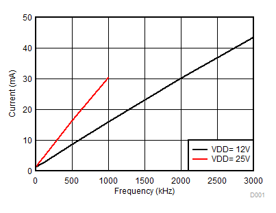
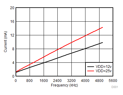
Figure 4. Per Channel Current Consumption vs. Frequency (No Load, VDD = 12 V or 25 V)
UCC21520-Q1 UCC21520A-Q1 10nF_I_5_17.gif
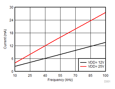
Figure 6. Per Channel Current Consumption (IVDDA/B) vs. Frequency (10-nF Load, VDD = 12 V or 25 V)
UCC21520-Q1 UCC21520A-Q1 IQ_5_17.gif
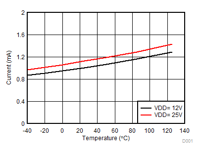
Figure 8. Per Channel (IVDDA/B) Quiescent Supply Current vs Temperature (No Load, Input Low, No Switching)
UCC21520-Q1 UCC21520A-Q1 RF_LOAD_NU.gif
Figure 10. Rising and Falling Times vs. Load (VDD = 12 V)
UCC21520-Q1 UCC21520A-Q1 PD_T_NU.gif
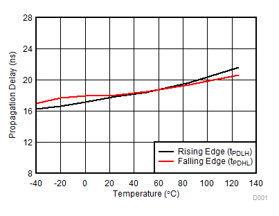
Figure 12. Propagation Delay vs. Temperature
UCC21520-Q1 UCC21520A-Q1 PWD.gif
Figure 14. Pulse Width Distortion vs. Temperature
UCC21520-Q1 UCC21520A-Q1 TDM_TEMP_NU.gif
Figure 16. Propagation Delay Matching (tDM) vs. Temperature
UCC21520-Q1 UCC21520A-Q1 D013_SLUSCO3.gif
Figure 18. VDD 5-V UVLO Threshold vs. Temperature
UCC21520-Q1 UCC21520A-Q1 UVLO_VDD_TEMP_5_17.gif
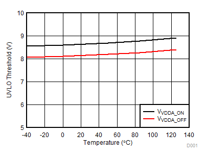
Figure 20. VDD 8-V UVLO Threshold vs. Temperature
UCC21520-Q1 UCC21520A-Q1 INDIS_LO_5_17.gif
Figure 22. IN/DIS Low Threshold
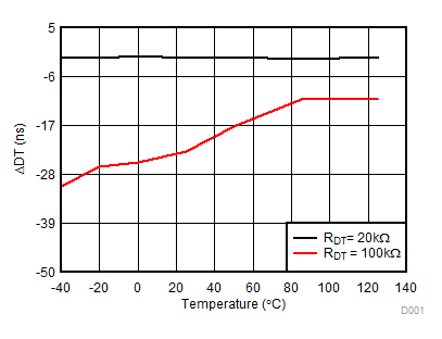
UCC21520-Q1 UCC21520A-Q1 DT_TEMP_NU.gif
Figure 24. Dead Time vs. Temperature (with RDT = 20 kΩ and 100 kΩ)
UCC21520-Q1 UCC21520A-Q1 Nu_SCOPE.gif
Figure 26. Typical Output Waveforms
UCC21520-Q1 UCC21520A-Q1 1nF_I_5_17.gif
Figure 5. Per Channel Current Consumption (IVDDA/B) vs. Frequency (1-nF Load, VDD = 12 V or 25 V)
UCC21520-Q1 UCC21520A-Q1 IVDD_TEMP_5_17.gif
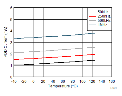
Figure 7. Per Channel (IVDDA/B) Supply Current Vs. Temperature (No Load, Different Switching Frequencies)
UCC21520-Q1 UCC21520A-Q1 Iq_IVCCI.gif
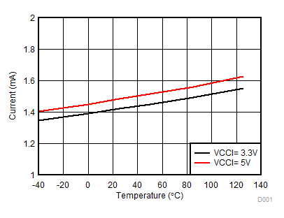
Figure 9. IVCCI Quiescent Supply Current vs Temperature (No Load, Input Low, No Switching)
UCC21520-Q1 UCC21520A-Q1 OUTR_5_17.gif
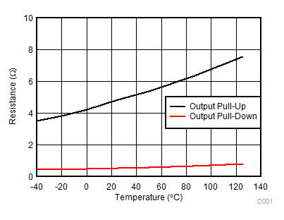
Figure 11. Output Resistance vs. Temperature
UCC21520-Q1 UCC21520A-Q1 PDVCC_NUNU.gif
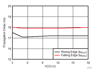
Figure 13. Propagation Delay vs. VCCI
UCC21520-Q1 UCC21520A-Q1 TDM_VDD_NU.gif
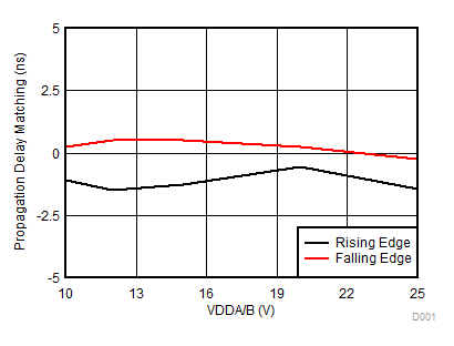
Figure 15. Propagation Delay Matching (tDM) vs. VDD
UCC21520-Q1 UCC21520A-Q1 D017_SLUSCO3.gif
Figure 17. VDD 5-V UVLO Hysteresis vs. Temperature
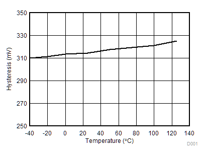
UCC21520-Q1 UCC21520A-Q1 VDD_HYS_5_17.gif
Figure 19. VDD 8-V UVLO Hysteresis vs. Temperature
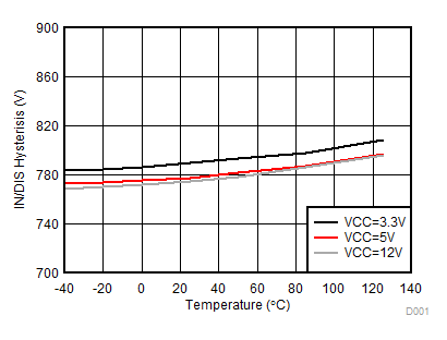
UCC21520-Q1 UCC21520A-Q1 INDIS_HYS_5_17.gif
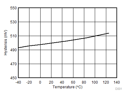
Figure 21. IN/DIS Hysteresis vs. Temperature
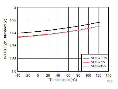
UCC21520-Q1 UCC21520A-Q1 INDIS_HI_5_17.gif
Figure 23. IN/DIS High Threshold
UCC21520-Q1 UCC21520A-Q1 DTM_TEMP_NU.gif
Figure 25. Dead Time Matching vs. Temperature (with RDT = 20 kΩ and 100 kΩ)