SLUSCJ9E June 2016 – December 2021 UCC21520
PRODUCTION DATA
- 1 Features
- 2 Applications
- 3 Description
- 4 Revision History
- 5 Description (continued)
- 6 Pin Configuration and Functions
-
7 Specifications
- 7.1 Absolute Maximum Ratings
- 7.2 ESD Ratings
- 7.3 Recommended Operating Conditions
- 7.4 Thermal Information
- 7.5 Power Ratings
- 7.6 Insulation Specifications
- 7.7 Safety-Related Certifications
- 7.8 Safety-Limiting Values
- 7.9 Electrical Characteristics
- 7.10 Switching Characteristics
- 7.11 Insulation Characteristics Curves
- 7.12 Typical Characteristics
- 8 Parameter Measurement Information
- 9 Detailed Description
-
10Application and Implementation
- 10.1 Application Information
- 10.2
Typical Application
- 10.2.1 Design Requirements
- 10.2.2
Detailed Design Procedure
- 10.2.2.1 Designing INA/INB Input Filter
- 10.2.2.2 Select External Bootstrap Diode and its Series Resistor
- 10.2.2.3 Gate Driver Output Resistor
- 10.2.2.4 Gate to Source Resistor Selection
- 10.2.2.5 Estimate Gate Driver Power Loss
- 10.2.2.6 Estimating Junction Temperature
- 10.2.2.7 Selecting VCCI, VDDA/B Capacitor
- 10.2.2.8 Dead Time Setting Guidelines
- 10.2.2.9 Application Circuits with Output Stage Negative Bias
- 10.2.3 Application Curves
- 11Power Supply Recommendations
- 12Layout
- 13Device and Documentation Support
- 14Mechanical, Packaging, and Orderable Information
Package Options
Mechanical Data (Package|Pins)
- DW|16
Thermal pad, mechanical data (Package|Pins)
- DW|16
Orderable Information
10.2.2.8 Dead Time Setting Guidelines
For power converter topologies utilizing half-bridges, the dead time setting between the top and bottom transistor is important for preventing shoot-through during dynamic switching.
The UCC21520 dead time specification in the electrical table is defined as the time interval from 90% of one channel’s falling edge to 10% of the other channel’s rising edge (see Figure 8-4). This definition ensures that the dead time setting is independent of the load condition, and guarantees linearity through manufacture testing. However, this dead time setting may not reflect the dead time in the power converter system, since the dead time setting is dependent on the external gate drive turn-on/off resistor, DC-Link switching voltage/current, as well as the input capacitance of the load transistor.
Here is a suggestion on how to select an appropriate dead time for UCC21520:
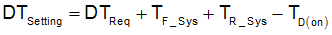
where
- DTsetting: UCC21520 dead time setting in ns, DTSetting = 10 × RDT(in kΩ).
- DTReq: System required dead time between the real VGS signal of the top and bottom switch with enough margin, or ZVS requirement.
- TF_Sys: In-system gate turn-off falling time at worst case of load, voltage/current conditions.
- TR_Sys: In-system gate turn-on rising time at worst case of load, voltage/current conditions.
- TD(on): Turn-on delay time, from 10% of the transistor gate signal to power transistor gate threshold.
In the example, DTSetting is set to 250 ns.
It should be noted that the UCC21520 dead time setting is decided by the DT pin configuration (See Section 9.4.2), and it cannot automatically fine-tune the dead time based on system conditions. It is recommended to parallel a ceramic capacitor, 2.2 nF or above, close to the DT pin with RDT to achieve better noise immunity.