SLUSDE1D November 2018 – February 2021 UCC21540 , UCC21540A , UCC21541 , UCC21542
PRODMIX
- 1 Features
- 2 Applications
- 3 Description
- 4 Revision History
- 5 Device Comparison Table
- 6 Pin Configuration and Functions
-
7 Specifications
- 7.1 Absolute Maximum Ratings
- 7.2 ESD Ratings
- 7.3 Recommended Operating Conditions
- 7.4 Thermal Information
- 7.5 Power Ratings
- 7.6 Insulation Specifications
- 7.7 Safety-Related Certifications
- 7.8 Safety-Limiting Values
- 7.9 Electrical Characteristics
- 7.10 Switching Characteristics
- 7.11 Insulation Characteristics Curves
- 7.12 Typical Characteristics
- 8 Parameter Measurement Information
- 9 Detailed Description
-
10Application and Implementation
- 10.1 Application Information
- 10.2
Typical Application
- 10.2.1 Design Requirements
- 10.2.2
Detailed Design Procedure
- 10.2.2.1 Designing INA/INB Input Filter
- 10.2.2.2 Select Dead Time Resistor and Capacitor
- 10.2.2.3 Select External Bootstrap Diode and its Series Resistor
- 10.2.2.4 Gate Driver Output Resistor
- 10.2.2.5 Gate to Source Resistor Selection
- 10.2.2.6 Estimating Gate Driver Power Loss
- 10.2.2.7 Estimating Junction Temperature
- 10.2.2.8 Selecting VCCI, VDDA/B Capacitor
- 10.2.2.9 Application Circuits with Output Stage Negative Bias
- 10.2.3 Application Curves
- 11Power Supply Recommendations
- 12Layout
- 13Device and Documentation Support
- 14Mechanical, Packaging, and Orderable Information
Package Options
Refer to the PDF data sheet for device specific package drawings
Mechanical Data (Package|Pins)
- DWK|14
- DW|16
Thermal pad, mechanical data (Package|Pins)
- DW|16
Orderable Information
10.2.2.3 Select External Bootstrap Diode and its Series Resistor
The bootstrap capacitor is charged by VDD through an external bootstrap diode every cycle when the low side transistor turns on. Charging the capacitor involves high-peak currents, and therefore transient power dissipation in the bootstrap diode may be significant. Conduction loss also depends on the diode’s forward voltage drop. Both the diode conduction losses and reverse recovery losses contribute to the total losses in the gate driver circuit.
When selecting external bootstrap diodes, TI recommends choosing high voltage, fast recovery diodes or SiC Schottky diodes with a low forward voltage drop and low junction capacitance in order to minimize the loss introduced by reverse recovery and related grounding noise bouncing. In the example, the DC-link voltage is 400 VDC. The voltage rating of the bootstrap diode should be higher than the DC-link voltage with a good margin. Therefore, a 600-V ultrafast diode, MURA160T3G, is chosen in this example.
A bootstrap resistor, RBOOT, is used to reduce the inrush current in DBOOT and limit the ramp up slew rate of voltage of VDDA-VSSA during each switching cycle, especially when the VSSA(SW) pin has an excessive negative transient voltage. The recommended value for RBOOT is between 1 Ω and 20 Ω depending on the diode used. In the example, a current limiting resistor of 2.7 Ω is selected to limit the inrush current of bootstrap diode. The estimated worst case peak current through DBoot is,
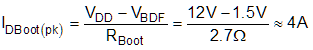
where
- VBDF is the estimated bootstrap diode forward voltage drop around 4 A.
Failure to limit the voltage to VDDx-VSSx to less than the Absolute Maximum Ratings of the FET and UCC2154x may result in permanent damage to the device in certain cases.