SLUSDO2C June   2020  – February 2021 UCC21540-Q1

PRODUCTION DATA  

  1. Features
  2. Applications
  3. Description
  4. Revision History
  5. Device Comparison Table
  6. Pin Configuration and Functions
    1.     UCC21540-Q1 Pin Functions
  7. Specifications
    1. 7.1  Absolute Maximum Ratings
    2. 7.2  ESD Ratings
    3. 7.3  Recommended Operating Conditions
    4. 7.4  Thermal Information
    5. 7.5  Power Ratings
    6. 7.6  Insulation Specifications
    7. 7.7  Safety-Related Certifications
    8. 7.8  Safety-Limiting Values
    9. 7.9  Electrical Characteristics
    10. 7.10 Switching Characteristics
    11. 7.11 Insulation Characteristics Curves
    12. 7.12 Typical Characteristics
  8. Parameter Measurement Information
    1. 8.1 Minimum Pulses
    2. 8.2 Propagation Delay and Pulse Width Distortion
    3. 8.3 Rising and Falling Time
    4. 8.4 Input and Disable Response Time
    5. 8.5 Programmable Dead Time
    6. 8.6 Power-up UVLO Delay to OUTPUT
    7. 8.7 CMTI Testing
  9. Detailed Description
    1. 9.1 Overview
    2. 9.2 Functional Block Diagram
    3. 9.3 Feature Description
      1. 9.3.1 VDD, VCCI, and Under Voltage Lock Out (UVLO)
      2. 9.3.2 Input and Output Logic Table
      3. 9.3.3 Input Stage
      4. 9.3.4 Output Stage
      5. 9.3.5 Diode Structure in the UCC21540-Q1
    4. 9.4 Device Functional Modes
      1. 9.4.1 Disable Pin
      2. 9.4.2 Programmable Dead Time (DT) Pin
        1. 9.4.2.1 DT Pin Tied to VCCI
        2. 9.4.2.2 Connecting a Programming Resistor between DT and GND Pins
  10. 10Application and Implementation
    1. 10.1 Application Information
    2. 10.2 Typical Application
      1. 10.2.1 Design Requirements
      2. 10.2.2 Detailed Design Procedure
        1. 10.2.2.1 Designing INA/INB Input Filter
        2. 10.2.2.2 Select Dead Time Resistor and Capacitor
        3. 10.2.2.3 Select External Bootstrap Diode and its Series Resistor
        4. 10.2.2.4 Gate Driver Output Resistor
        5. 10.2.2.5 Gate to Source Resistor Selection
        6. 10.2.2.6 Estimating Gate Driver Power Loss
        7. 10.2.2.7 Estimating Junction Temperature
        8. 10.2.2.8 Selecting VCCI, VDDA/B Capacitor
          1. 10.2.2.8.1 Selecting a VCCI Capacitor
          2. 10.2.2.8.2 Selecting a VDDA (Bootstrap) Capacitor
          3. 10.2.2.8.3 Select a VDDB Capacitor
        9. 10.2.2.9 Application Circuits with Output Stage Negative Bias
      3. 10.2.3 Application Curves
  11. 11Power Supply Recommendations
  12. 12Layout
    1. 12.1 Layout Guidelines
      1. 12.1.1 Component Placement Considerations
      2. 12.1.2 Grounding Considerations
      3. 12.1.3 High-Voltage Considerations
      4. 12.1.4 Thermal Considerations
    2. 12.2 Layout Example
  13. 13Device and Documentation Support
    1. 13.1 Documentation Support
      1. 13.1.1 Related Documentation
    2. 13.2 Receiving Notification of Documentation Updates
    3. 13.3 Support Resources
    4. 13.4 Trademarks
    5. 13.5 Electrostatic Discharge Caution
    6. 13.6 Glossary
  14. 14Mechanical, Packaging, and Orderable Information

Package Options

Mechanical Data (Package|Pins)
Thermal pad, mechanical data (Package|Pins)
Orderable Information

Typical Characteristics

VDDA = VDDB = 12 V, VCCI = 3.3 V or 5.0 V, DT pin tied to VCCI, TA = 25°C, CL = 0 pF unless otherwise noted.
GUID-49180F9C-64BB-41CF-B17D-E52ECE0A73DF-low.gif
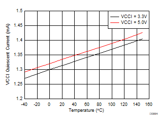
No Load INA = INB = GND
Figure 7-4 VCCI Quiescent Current
GUID-12883430-149C-4E8E-A298-D59E220076FE-low.gif
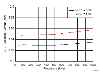
Figure 7-6 VCCI Operating Current vs. Frequency
GUID-C53B938F-AABD-4933-BAEF-BA87B310C746-low.gif
No Load
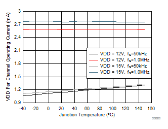
Figure 7-8 VDD Per Channel Operating Current - IVDDA/B
GUID-85EB26CE-61C6-4C5B-9D6E-744F321BA50D-low.gif
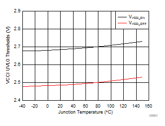
Figure 7-10 VCCI UVLO Threshold Voltage
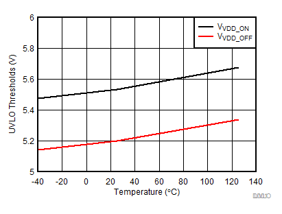
GUID-51C6757E-7BDC-4381-B6F8-631B82170635-low.gifFigure 7-12 5-V VDD UVLO Threshold Voltage
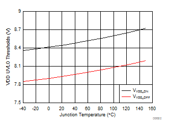
GUID-A130FF33-C053-4A4A-BC0B-1A30CBFE2802-low.gif
Figure 7-14 8-V VDD UVLO Threshold Voltage
GUID-85E60498-8189-4B5F-B761-6031B9DBDDBA-low.gif
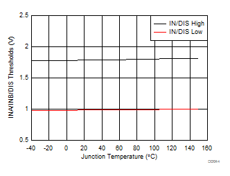
Figure 7-16 INA/INB/DIS High and Low Threshold Voltage
GUID-74A5701B-A4CB-4275-90C7-301FE103A78D-low.gif
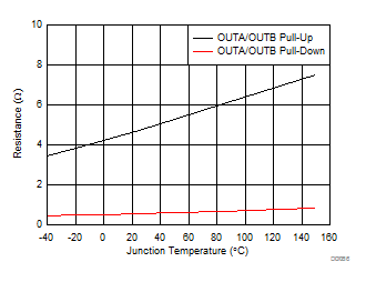
Figure 7-18 OUT Pullup and Pulldown Resistance
GUID-C77A0456-4166-474A-928C-476B09509122-low.gif
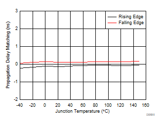
Figure 7-20 Propagation Delay Matching, Rising and Falling Edge
GUID-0266870B-74DB-4B50-AF4B-8B9F7238C6F9-low.gif
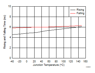
CL = 1.8 nF
Figure 7-22 Rise Time and Fall Time
GUID-B59BF052-9E98-43B4-9FE3-3A25338CA993-low.gif
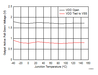
Figure 7-24 OUTPUT Active Pulldown Voltage
GUID-BF19051A-A02C-445A-9D63-F1B3DFD9156C-low.gif
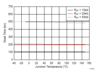
Figure 7-26 Dead Time Temperature Drift
GUID-4C08EEAB-E919-4A2B-921D-AF4F9775B40F-low.gif
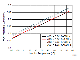
Figure 7-5 VCCI Operating Current - IVCCI
GUID-E964C293-05D0-4289-9D83-12E818DCE44C-low.gif
No Load INA = INB = GND
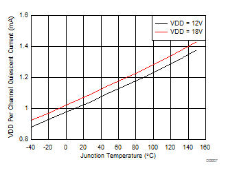
Figure 7-7 VDD Per Channel Quiescent Current (IVDDA, IVDDB)
GUID-A0E993EC-EC64-46AC-B93E-624A1BEC7F52-low.gif
No Load INA and INB both switching
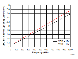
Figure 7-9 Per Channel Operating Current (IVDDA/B) vs. Frequency
GUID-EF34E00E-FD41-423B-A575-3E94A905745E-low.gif
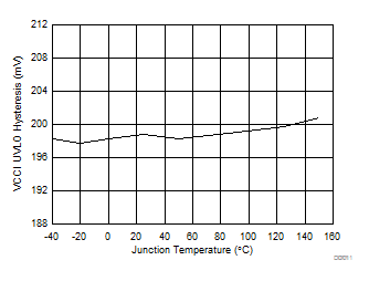
Figure 7-11 VCCI UVLO Threshold Hysteresis Voltage
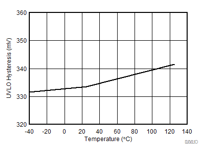
GUID-2902E0F6-8A66-412E-9A86-8531F0B78545-low.gifFigure 7-13 5-V VDD UVLO Hysteresis Voltage
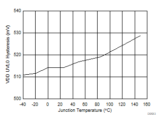
GUID-5B98EC76-E437-4DD4-954F-63BB8067CD21-low.gif
Figure 7-15 8-V VDD UVLO Threshold Hysteresis Voltage
GUID-D485A126-87B9-4ABF-9344-62271C9DEDDE-low.gif
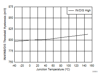
Figure 7-17 INA/INB/DIS High and Low Threshold Hysteresis
GUID-97559F0C-FFDD-46C1-80C1-AD28831C4F36-low.gif
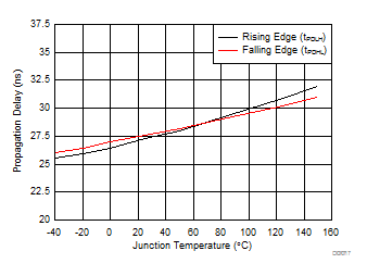
Figure 7-19 Propagation Delay, Rising and Falling Edge
GUID-6ED522F5-98ED-4C79-8308-38824A14662C-low.gif
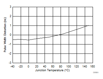
tPDLH – tPDHL
Figure 7-21 Pulse Width Distortion
GUID-2D9DC15B-BB9E-4D46-8463-9C9E7F29FADD-low.gif
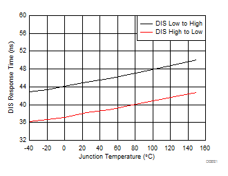
Figure 7-23 DISABLE Response Time
GUID-EB0A3AF3-F3DD-4EC4-8FB0-5BAEA0FA8FB1-low.gif
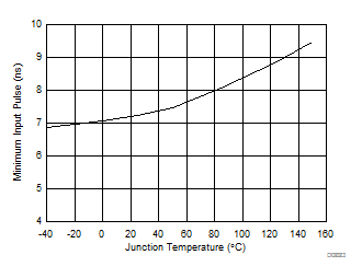
Figure 7-25 Minimum Pulse that Changes Output
GUID-AFA0BA9C-A205-4F90-8779-19C2F25EA03C-low.gif
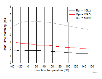
Figure 7-27 Dead Time Matching