SLUSDO2C June 2020 – February 2021 UCC21540-Q1
PRODUCTION DATA
- 1 Features
- 2 Applications
- 3 Description
- 4 Revision History
- 5 Device Comparison Table
- 6 Pin Configuration and Functions
-
7 Specifications
- 7.1 Absolute Maximum Ratings
- 7.2 ESD Ratings
- 7.3 Recommended Operating Conditions
- 7.4 Thermal Information
- 7.5 Power Ratings
- 7.6 Insulation Specifications
- 7.7 Safety-Related Certifications
- 7.8 Safety-Limiting Values
- 7.9 Electrical Characteristics
- 7.10 Switching Characteristics
- 7.11 Insulation Characteristics Curves
- 7.12 Typical Characteristics
- 8 Parameter Measurement Information
- 9 Detailed Description
-
10Application and Implementation
- 10.1 Application Information
- 10.2
Typical Application
- 10.2.1 Design Requirements
- 10.2.2
Detailed Design Procedure
- 10.2.2.1 Designing INA/INB Input Filter
- 10.2.2.2 Select Dead Time Resistor and Capacitor
- 10.2.2.3 Select External Bootstrap Diode and its Series Resistor
- 10.2.2.4 Gate Driver Output Resistor
- 10.2.2.5 Gate to Source Resistor Selection
- 10.2.2.6 Estimating Gate Driver Power Loss
- 10.2.2.7 Estimating Junction Temperature
- 10.2.2.8 Selecting VCCI, VDDA/B Capacitor
- 10.2.2.9 Application Circuits with Output Stage Negative Bias
- 10.2.3 Application Curves
- 11Power Supply Recommendations
- 12Layout
- 13Device and Documentation Support
- 14Mechanical, Packaging, and Orderable Information
Package Options
Mechanical Data (Package|Pins)
- DWK|14
Thermal pad, mechanical data (Package|Pins)
Orderable Information
10.2.3 Application Curves
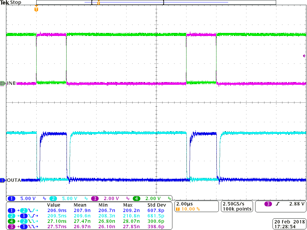
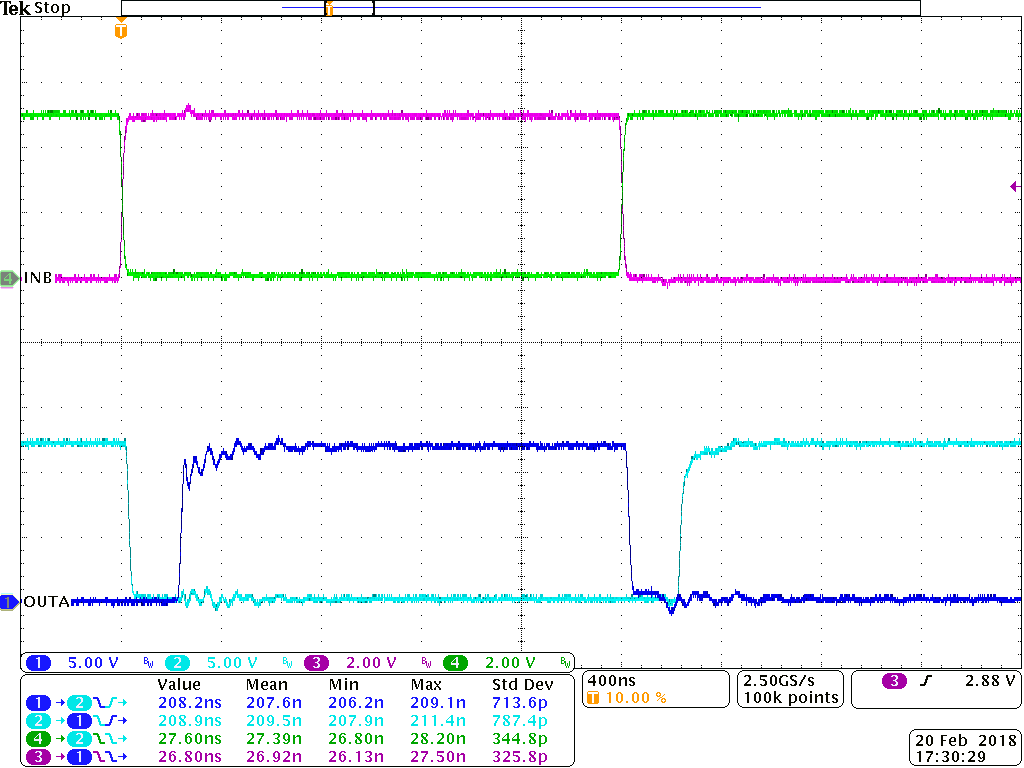
Figure 10-5 and Figure 10-6 shows the bench test waveforms for the design example shown in Figure 10-1 under these conditions: VCC = 5.0 V, VDD = 12 V, fSW = 100 kHz, VDC-Link = 400 V.
Channel 1 (Blue): Gate-source signal on the high side power transistor.
Channel 2 (Cyan): Gate-source signal on the low side power transistor.
Channel 3 (Pink): INA pin signal.
Channel 4 (Green): INB pin signal.
In Figure 10-5, INA and INB are sent complimentary 3.3-V, 20%/80% duty-cycle signals. The gate drive signals on the power transistor have a 200-ns dead time with 400V high voltage on the DC-Link, shown in the measurement section of Figure 10-5. Note that with high voltage present, lower bandwidth differential probes are required, which limits the achievable accuracy of the measurement.
Figure 10-6 shows a zoomed-in version of the waveform of Figure 10-5, with measurements for propagation delay and dead time. Importantly, the output waveform is measured between the power transistors’ gate and source pins, and is not measured directly from the driver OUTA and OUTB pins.

