SLUSDE1D November 2018 – February 2021 UCC21540 , UCC21540A , UCC21541 , UCC21542
PRODMIX
- 1 Features
- 2 Applications
- 3 Description
- 4 Revision History
- 5 Device Comparison Table
- 6 Pin Configuration and Functions
-
7 Specifications
- 7.1 Absolute Maximum Ratings
- 7.2 ESD Ratings
- 7.3 Recommended Operating Conditions
- 7.4 Thermal Information
- 7.5 Power Ratings
- 7.6 Insulation Specifications
- 7.7 Safety-Related Certifications
- 7.8 Safety-Limiting Values
- 7.9 Electrical Characteristics
- 7.10 Switching Characteristics
- 7.11 Insulation Characteristics Curves
- 7.12 Typical Characteristics
- 8 Parameter Measurement Information
- 9 Detailed Description
-
10Application and Implementation
- 10.1 Application Information
- 10.2
Typical Application
- 10.2.1 Design Requirements
- 10.2.2
Detailed Design Procedure
- 10.2.2.1 Designing INA/INB Input Filter
- 10.2.2.2 Select Dead Time Resistor and Capacitor
- 10.2.2.3 Select External Bootstrap Diode and its Series Resistor
- 10.2.2.4 Gate Driver Output Resistor
- 10.2.2.5 Gate to Source Resistor Selection
- 10.2.2.6 Estimating Gate Driver Power Loss
- 10.2.2.7 Estimating Junction Temperature
- 10.2.2.8 Selecting VCCI, VDDA/B Capacitor
- 10.2.2.9 Application Circuits with Output Stage Negative Bias
- 10.2.3 Application Curves
- 11Power Supply Recommendations
- 12Layout
- 13Device and Documentation Support
- 14Mechanical, Packaging, and Orderable Information
Package Options
Refer to the PDF data sheet for device specific package drawings
Mechanical Data (Package|Pins)
- DWK|14
- DW|16
Thermal pad, mechanical data (Package|Pins)
- DW|16
Orderable Information
10.2.2.6 Estimating Gate Driver Power Loss
The total loss, PG, in the gate driver subsystem includes the power losses of the UCC2154x (PGD) and the power losses in the peripheral circuitry, such as the external gate drive resistor. Bootstrap diode loss is not included in PG and not discussed in this section.
PGD is the key power loss which determines the thermal safety-related limits of the UCC2154x , and it can be estimated by calculating losses from several components.
The first component is the static power loss, PGDQ, which includes quiescent power loss on the driver as well as driver self-power consumption when operating with a certain switching frequency. PGDQ is measured on the bench with no load connected to OUTA and OUTB at a given VCCI, VDDA/VDDB, switching frequency and ambient temperature. Figure 7-6 and Figure 7-9 show the operating current consumption vs. operating frequency with no load. In this example, VVCCI = 5 V and VVDD = 12 V. The current on each power supply, with INA/INB switching from 0 V to 3.3 V at 100 kHz is measured to be IVCCI ≈ 2.5 mA, and IVDDA = IVDDB ≈ 1.5 mA. Therefore, the PGDQ can be calculated with

The second component is switching operation loss, PGDO, with a given load capacitance which the driver charges and discharges the load during each switching cycle. Total dynamic loss due to load switching, PGSW, can be estimated with

where
- QG is the gate charge of the power transistor.
If a split rail is used to turn on and turn off, then VDD is going to be equal to difference between the positive rail to the negative rail.
So, for this example application:

QG represents the total gate charge of the power transistor switching 480 V at 14 A provided by the datasheet, and is subject to change with different testing conditions. The UCC2154x gate driver loss on the output stage, PGDO, is part of PGSW. PGDO will be equal to PGSW if the external gate driver resistances are zero, and all the gate driver loss is dissipated inside the UCC2154x. If there are external turn-on and turn-off resistances, the total loss will be distributed between the gate driver pull-up/down resistances and external gate resistances. Importantly, the pull-up/down resistance is a linear and fixed resistance if the source/sink current is not saturated to 4 A/6 A, however, it will be non-linear if the source/sink current is saturated. Therefore, PGDO is different in these two scenarios.
Case 1 - Linear Pull-Up/Down Resistor:
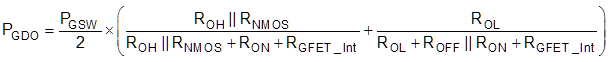
In this design example, all the predicted source/sink currents are less than 4 A/6 A, therefore, the UCC2154x gate driver loss can be estimated with:

Case 2 - Nonlinear Pull-Up/Down Resistor:
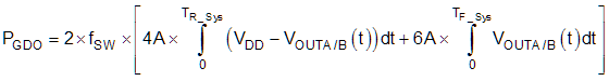
where
- VOUTA/B(t) is the gate driver OUTA and OUTB pin voltage during the turn on and off transient, and it can be simplified that a constant current source (4 A at turn-on and 6 A at turn-off) is charging/discharging a load capacitor. Then, the VOUTA/B(t) waveform will be linear and the TR_Sys and TF_Sys can be easily predicted.
For some scenarios, if only one of the pull-up or pull-down circuits is saturated and another one is not, the PGDO will be a combination of Case 1 and Case 2, and the equations can be easily identified for the pull-up and pull-down based on the above discussion. Therefore, total gate driver loss dissipated in the gate driver UCC2154x PGD, is:

which is equal to 127 mW in the design example.