SLUSDE1D November 2018 – February 2021 UCC21540 , UCC21540A , UCC21541 , UCC21542
PRODMIX
- 1 Features
- 2 Applications
- 3 Description
- 4 Revision History
- 5 Device Comparison Table
- 6 Pin Configuration and Functions
-
7 Specifications
- 7.1 Absolute Maximum Ratings
- 7.2 ESD Ratings
- 7.3 Recommended Operating Conditions
- 7.4 Thermal Information
- 7.5 Power Ratings
- 7.6 Insulation Specifications
- 7.7 Safety-Related Certifications
- 7.8 Safety-Limiting Values
- 7.9 Electrical Characteristics
- 7.10 Switching Characteristics
- 7.11 Insulation Characteristics Curves
- 7.12 Typical Characteristics
- 8 Parameter Measurement Information
- 9 Detailed Description
-
10Application and Implementation
- 10.1 Application Information
- 10.2
Typical Application
- 10.2.1 Design Requirements
- 10.2.2
Detailed Design Procedure
- 10.2.2.1 Designing INA/INB Input Filter
- 10.2.2.2 Select Dead Time Resistor and Capacitor
- 10.2.2.3 Select External Bootstrap Diode and its Series Resistor
- 10.2.2.4 Gate Driver Output Resistor
- 10.2.2.5 Gate to Source Resistor Selection
- 10.2.2.6 Estimating Gate Driver Power Loss
- 10.2.2.7 Estimating Junction Temperature
- 10.2.2.8 Selecting VCCI, VDDA/B Capacitor
- 10.2.2.9 Application Circuits with Output Stage Negative Bias
- 10.2.3 Application Curves
- 11Power Supply Recommendations
- 12Layout
- 13Device and Documentation Support
- 14Mechanical, Packaging, and Orderable Information
Package Options
Refer to the PDF data sheet for device specific package drawings
Mechanical Data (Package|Pins)
- DWK|14
- DW|16
Thermal pad, mechanical data (Package|Pins)
- DW|16
Orderable Information
10.2.2.8.2 Selecting a VDDA (Bootstrap) Capacitor
A VDDA capacitor, also referred to as a bootstrap capacitor in bootstrap power supply configurations, allows for gate drive current transients up to 4-A, the source peak current, and needs to maintain a stable gate drive voltage for the power transistor.
The total charge needed per switching cycle can be estimated with
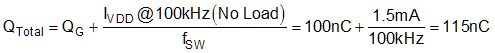
where
- QTotal: Total charge needed
- QG: Gate charge of the power transistor.
- IVDD: The channel self-current consumption with no load at 100kHz.
- fSW: The switching frequency of the gate driver
Therefore, the absolute minimum CBoot requirement is:
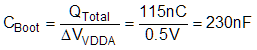
where
- ΔVVDDA is the voltage ripple at VDDA, which is 0.5 V in this example.
In practice, the value of CBoot is greater than the calculated value. This allows for the capacitance shift caused by the DC bias voltage and for situations where the power stage would otherwise skip pulses due to load transients. Therefore, it is recommended to include a margin in the CBoot value and place it as close to the VDD and VSS pins as possible. A 50-V 1-µF capacitor is chosen in this example.

Care should be taken when selecting the bootstrap capacitor to ensure that the VDD to VSS voltage does not drop below the recommended minimum operating level listed in section 6.3. The value of the bootstrap capacitor should be sized such that it can supply the initial charge to switch the power device, and then continuously supply the gate driver quiescent current for the duration of the high-side on-time.
If the high-side supply voltage drops below the UVLO falling threshold, the high-side gate driver output will turn off and switch the power device off. Uncontrolled hard-switching of power devices can cause high di/dt and high dv/dt transients on the output of the driver and may result in permanent damage to the device.
To further lower the AC impedance for a wide frequency range, it is recommended to have bypass capacitor placed very close to VDDx - VSSx pins with a low ESL/ESR. In this example a 100 nF, X7R ceramic capacitor, is placed in parallel with CBoot to optimize the transient performance.
Too large CBOOT is not good. CBOOT may not be charged within the first few cycles and VBOOT could stay below UVLO. As a result, the high-side FET does not follow input signal command. Also during initial CBOOT charging cycles, the bootstrap diode has highest reverse recovery current and losses.