SLUSDM7A April 2020 – May 2020 UCC21736-Q1
PRODUCTION DATA.
- 1 Features
- 2 Applications
- 3 Description
- 4 Revision History
- 5 Pin Configuration and Functions
-
6 Specifications
- 6.1 Absolute Maximum Ratings
- 6.2 ESD Ratings
- 6.3 Recommended Operating Conditions
- 6.4 Thermal Information
- 6.5 Power Ratings
- 6.6 Insulation Specifications
- 6.7 Safety-Related Certifications
- 6.8 Safety Limiting Values
- 6.9 Electrical Characteristics
- 6.10 Switching Characteristics
- 6.11 Insulation Characteristics Curves
- 6.12 Typical Characteristics
- 7 Parameter Measurement Information
-
8 Detailed Description
- 8.1 Overview
- 8.2 Functional Block Diagram
- 8.3
Feature Description
- 8.3.1 Power Supply
- 8.3.2 Driver Stage
- 8.3.3 VCC, VDD and VEE Undervoltage Lockout (UVLO)
- 8.3.4 Active Pulldown
- 8.3.5 Short Circuit Clamping
- 8.3.6 External Active Miller Clamp
- 8.3.7 Overcurrent and Short Circuit Protection
- 8.3.8 Fault (FLT, Reset and Enable (RST/EN)
- 8.3.9 ASC Protection and APWM Monitor
- 8.4 Device Functional Modes
-
9 Applications and Implementation
- 9.1 Application Information
- 9.2
Typical Application
- 9.2.1 Design Requirements
- 9.2.2
Detailed Design Procedure
- 9.2.2.1 Input filters for IN+, IN- and RST/EN
- 9.2.2.2 PWM Interlock of IN+ and IN-
- 9.2.2.3 FLT, RDY and RST/EN Pin Circuitry
- 9.2.2.4 RST/EN Pin Control
- 9.2.2.5 Turn on and turn off gate resistors
- 9.2.2.6 External Active Miller Clamp
- 9.2.2.7 Overcurrent and Short Circuit Protection
- 9.2.2.8 Higher Output Current Using an External Current Buffer
- 9.2.3 Application Curves
- 10Power Supply Recommendations
- 11Layout
- 12Device and Documentation Support
- 13Mechanical, Packaging, and Orderable Information
Package Options
Mechanical Data (Package|Pins)
- DW|16
Thermal pad, mechanical data (Package|Pins)
- DW|16
Orderable Information
8.3.7 Overcurrent and Short Circuit Protection
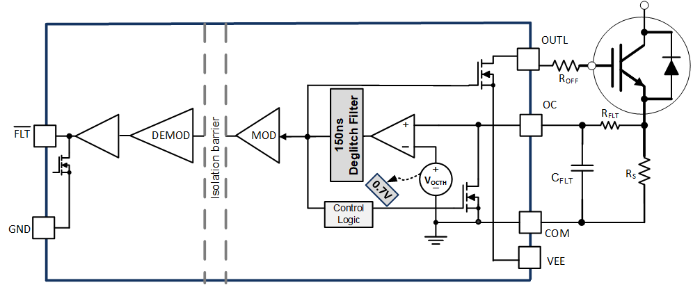
The UCC21736-Q1 implements a fast overcurrent and short circuit protection feature to protect the SiC MOSFET or IGBT from catastrophic breakdown during fault. The OC pin of the device has a typical 0.7V threshold with respect to COM, source or emitter of the power semiconductor. When the input is in floating condition, or the output is held in low state, the OC pin is pulled down by an internal MOSFET and held in LOW state, which prevents the overcurrent and short circuit fault from false triggering. The OC pin is in high-impedance state when the output is in high state, which means the overcurrent and short circuit protection feature only works when the power semiconductor is in on state. The internal pulldown MOSFET helps to discharge the voltage of OC pin when the power semiconductor is turned off.
The overcurrent and short circuit protection feature can be used to SiC MOSFET module or IGBT module with SenseFET, traditional desaturation circuit and shunt resistor in series with the power loop for lower power applications. For SiC MOSFET module or IGBT module with SenseFET, the SenseFET integrated in the module can scale down the drain current or collector current. With an external high precision sense resistor, the drain current or collector current can be accurately measured. If the voltage of the sensed resistor higher than the overcurrent threshold VOCTH is detected, the soft turn-off is initiated. A fault will be reported to the input side FLT pin to DSP/MCU. The output is held to LOW after the fault is detected, and can only be reset by the RST/EN pin. The state-of-art overcurrent and short circuit detection time helps to ensure a short shutdown time for SiC MOSFET and IGBT.
The overcurrent and short circuit protection feature can also be paired with desaturation circuit and shunt resistors. The DESAT threshold can be programmable in this case, which increases the versatility of the device. Detailed application diagrams of desaturation circuit and shunt resistor will be given in .
- High current and high dI/dt during the overcurrent and short circuit fault can cause a voltage bounce on shunt resistor’s parasitic inductance and board layout parasitic, which results in false trigger of OC pin. High precision, low ESL and small value resistor must be used in this approach.
- Shunt resistor approach is not recommended for high power applications and short circuit protection of the low power applications.
The detailed applications of the overcurrent and short circuit feature will be discussed in the Application and Implementation section.
 Figure 43. Overcurrent and Short Circuit Protection