SLUSEM3B March 2022 – January 2023 UCC21737-Q1
PRODUCTION DATA
- 1 Features
- 2 Applications
- 3 Description
- 4 Revision History
- 5 Pin Configuration and Functions
-
6 Specifications
- 6.1 Absolute Maximum Ratings
- 6.2 ESD Ratings
- 6.3 Recommended Operating Conditions
- 6.4 Thermal Information
- 6.5 Power Ratings
- 6.6 Insulation Specifications
- 6.7 Safety Limiting Values
- 6.8 Electrical Characteristics
- 6.9 Switching Characteristics
- 6.10 Insulation Characteristics Curves
- 6.11 Typical Characteristics
- 7 Parameter Measurement Information
-
8 Detailed Description
- 8.1 Overview
- 8.2 Functional Block Diagram
- 8.3
Feature Description
- 8.3.1 Power Supply
- 8.3.2 Driver Stage
- 8.3.3 VCC, VDD, and VEE Undervoltage Lockout (UVLO)
- 8.3.4 Active Pulldown
- 8.3.5 Short Circuit Clamping
- 8.3.6 External Active Miller Clamp
- 8.3.7 Overcurrent and Short Circuit Protection
- 8.3.8 Soft Turn-off
- 8.3.9 Fault (FLT), Reset, and Enable (RST/EN)
- 8.3.10 ASC Support and APWM Monitor
- 8.4 Device Functional Modes
-
9 Applications and Implementation
- 9.1 Application Information
- 9.2
Typical Application
- 9.2.1 Design Requirements
- 9.2.2
Detailed Design Procedure
- 9.2.2.1 Input Filters for IN+, IN-, and RST/EN
- 9.2.2.2 PWM Interlock of IN+ and IN-
- 9.2.2.3 FLT, RDY, and RST/EN Pin Circuitry
- 9.2.2.4 RST/EN Pin Control
- 9.2.2.5 Turnon and Turnoff Gate Resistors
- 9.2.2.6 External Active Miller Clamp
- 9.2.2.7 Overcurrent and Short Circuit Protection
- 9.2.2.8 Higher Output Current Using an External Current Buffer
- 9.2.3 Application Curves
- 10Power Supply Recommendations
- 11Layout
- 12Device and Documentation Support
- 13Mechanical, Packaging, and Orderable Information
Package Options
Mechanical Data (Package|Pins)
- DW|16
Thermal pad, mechanical data (Package|Pins)
- DW|16
Orderable Information
9.2.2.7.2 Protection Based on Desaturation Circuit
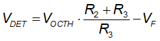
For SiC MOSFET and IGBT modules without SenseFET, the desaturation (DESAT) circuit is the most popular circuit which is adopted for overcurrent and short circuit protection. The circuit consists of a current source, a resistor, a blanking capacitor and a diode. Normally the current source is provided from the gate driver, when the device turns on, a current source charges the blanking capacitor and the diode forward biased. During normal operation, the capacitor voltage is clamped by the switch VCE voltage. When a short circuit happens, the capacitor voltage is quickly charged to the threshold voltage which triggers device shutdown. For the UCC21737-Q1, the OC pin does not feature an internal current source. The current source should be generated externally from the output power supply. When UCC21737-Q1 is in the OFF state, the OC pin is pulled down by an internal MOSFET, which creates an offset voltage on the OC pin. By choosing R1 and R2 significantly higher than the pulldown resistance of the internal MOSFET, the offset can be ignored. When the UCC21737-Q1 is in the ON state, the OC pin is high impedance. The current source is generated by the output power supply VDD and the external resistor divider R1, R2, and R3. The overcurrent detection threshold voltage of the IGBT is:
The blanking time of the detection circuit is:
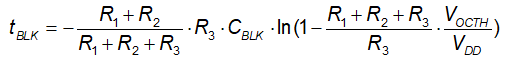
Where:
- VOCTH is the detection threshold voltage of the gate driver
- R1, R2, and R3 are the resistances of the voltage divider
- CBLK is the blanking capacitor
- VF is the forward voltage of the high voltage diode DHV
The modified desaturation circuit has all the benefits of the conventional desaturation circuit. The circuit has negligible power loss and is easy to implement. The detection threshold voltage of IGBT and blanking time can be programmed by external components. Different with the conventional desaturation circuit, the overcurrent detection threshold voltage of the IGBT can be modified to any voltage level, either higher or lower than the detection threshold voltage of the driver. A parallel schottky diode can be connected between the OC and COM pins to prevent negative voltage on the OC pin in a noisy system. Since the desaturation circuit measures the VCE of the IGBT or VDS of the SiC MOSFET, not directly the current, the accuracy of the protection is not as high as the SenseFET based protection method. The current threshold cannot be accurately controlled in the protection.
 Figure 9-9 Overcurrent and Short Circuit Protection Based on Desaturation Circuit