SLUSEM3B March 2022 – January 2023 UCC21737-Q1
PRODUCTION DATA
- 1 Features
- 2 Applications
- 3 Description
- 4 Revision History
- 5 Pin Configuration and Functions
-
6 Specifications
- 6.1 Absolute Maximum Ratings
- 6.2 ESD Ratings
- 6.3 Recommended Operating Conditions
- 6.4 Thermal Information
- 6.5 Power Ratings
- 6.6 Insulation Specifications
- 6.7 Safety Limiting Values
- 6.8 Electrical Characteristics
- 6.9 Switching Characteristics
- 6.10 Insulation Characteristics Curves
- 6.11 Typical Characteristics
- 7 Parameter Measurement Information
-
8 Detailed Description
- 8.1 Overview
- 8.2 Functional Block Diagram
- 8.3
Feature Description
- 8.3.1 Power Supply
- 8.3.2 Driver Stage
- 8.3.3 VCC, VDD, and VEE Undervoltage Lockout (UVLO)
- 8.3.4 Active Pulldown
- 8.3.5 Short Circuit Clamping
- 8.3.6 External Active Miller Clamp
- 8.3.7 Overcurrent and Short Circuit Protection
- 8.3.8 Soft Turn-off
- 8.3.9 Fault (FLT), Reset, and Enable (RST/EN)
- 8.3.10 ASC Support and APWM Monitor
- 8.4 Device Functional Modes
-
9 Applications and Implementation
- 9.1 Application Information
- 9.2
Typical Application
- 9.2.1 Design Requirements
- 9.2.2
Detailed Design Procedure
- 9.2.2.1 Input Filters for IN+, IN-, and RST/EN
- 9.2.2.2 PWM Interlock of IN+ and IN-
- 9.2.2.3 FLT, RDY, and RST/EN Pin Circuitry
- 9.2.2.4 RST/EN Pin Control
- 9.2.2.5 Turnon and Turnoff Gate Resistors
- 9.2.2.6 External Active Miller Clamp
- 9.2.2.7 Overcurrent and Short Circuit Protection
- 9.2.2.8 Higher Output Current Using an External Current Buffer
- 9.2.3 Application Curves
- 10Power Supply Recommendations
- 11Layout
- 12Device and Documentation Support
- 13Mechanical, Packaging, and Orderable Information
Package Options
Mechanical Data (Package|Pins)
- DW|16
Thermal pad, mechanical data (Package|Pins)
- DW|16
Orderable Information
9.2.2.8 Higher Output Current Using an External Current Buffer
To increase the IGBT gate drive current, a noninverting current buffer (such as the NPN/PNP buffer shown in Figure 9-11) can be used. Inverting types are not compatible with the desaturation fault protection circuitry and must be avoided. The MJD44H11/MJD45H11 pair is appropriate for peak currents up to 15 A, the D44VH10/ D45VH10 pair is for up to a 20-A peak.
In the case of an overcurrent detection, a soft turn off (STO) is activated. External components must be added to implement STO instead of normal turn-off speed when an external buffer is used. CSTO sets the timing for soft turn off and RSTO limits the inrush current to below the current rating of the internal FET (10 A). RSTO should be at least (VDD-VEE)/10. The soft turn-off timing is determined by the internal current source of 400 mA and the capacitor CSTO. CSTO is calculated using Equation 13.
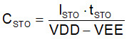
- ISTO is the the internal STO current source, 400 mA
- tSTO is the desired STO timing
 Figure 9-11 Current Buffer for Increased Drive Strength