SLUSEM9 September 2022 UCC21755-Q1
PRODUCTION DATA
- 1 Features
- 2 Applications
- 3 Description
- 4 Revision History
- 5 Pin Configuration and Functions
-
6 Specifications
- 6.1 Absolute Maximum Ratings
- 6.2 ESD Ratings
- 6.3 Recommended Operating Conditions
- 6.4 Thermal Information
- 6.5 Power Ratings
- 6.6 Insulation Specifications
- 6.7 Safety Limiting Values
- 6.8 Electrical Characteristics
- 6.9 Switching Characteristics
- 6.10 Insulation Characteristics Curves
- 6.11 Typical Characteristics
- 7 Parameter Measurement Information
-
8 Detailed Description
- 8.1 Overview
- 8.2 Functional Block Diagram
- 8.3
Feature Description
- 8.3.1 Power Supply
- 8.3.2 Driver Stage
- 8.3.3 VCC and VDD Undervoltage Lockout (UVLO)
- 8.3.4 Active Pulldown
- 8.3.5 Short Circuit Clamping
- 8.3.6 Internal Active Miller Clamp
- 8.3.7 Desaturation (DESAT) Protection
- 8.3.8 Soft Turn-Off
- 8.3.9 Fault (FLT), Reset and Enable (RST/EN)
- 8.3.10 Isolated Analog to PWM Signal Function
- 8.4 Device Functional Modes
-
9 Applications and Implementation
- 9.1 Application Information
- 9.2
Typical Application
- 9.2.1 Design Requirements
- 9.2.2
Detailed Design Procedure
- 9.2.2.1 Input Filters for IN+, IN- and RST/EN
- 9.2.2.2 PWM Interlock of IN+ and IN-
- 9.2.2.3 FLT, RDY, and RST/EN Pin Circuitry
- 9.2.2.4 RST/EN Pin Control
- 9.2.2.5 Turn-On and Turn-Off Gate Resistors
- 9.2.2.6 Overcurrent and Short Circuit Protection
- 9.2.2.7 Isolated Analog Signal Sensing
- 9.2.2.8 Higher Output Current Using an External Current Buffer
- 9.2.3 Application Curves
- 10Power Supply Recommendations
- 11Layout
- 12Device and Documentation Support
- 13Mechanical, Packaging, and Orderable Information
Package Options
Mechanical Data (Package|Pins)
- DW|16
Thermal pad, mechanical data (Package|Pins)
- DW|16
Orderable Information
9.2.2.8 Higher Output Current Using an External Current Buffer
To increase the IGBT gate drive current, a non-inverting current buffer (such as the NPN/PNP buffer shown in Figure 9-13) can be used. Inverting types are not compatible with the desaturation fault protection circuitry and must be avoided. The MJD44H11/MJD45H11 pair is appropriate for peak currents up to 15 A, the D44VH10/ D45VH10 pair is up to 20-A peak.
In the case of an overcurrent detection, the soft turn-off (STO) is activated. External components must be added to implement STO instead of normal turn-off speed when an external buffer is used. CSTO sets the timing for soft turn-off and RSTO limits the inrush current to below the current rating of the internal FET (10A). RSTO should be at least (VDD-VEE)/10. The soft turn-off timing is determined by the internal current source of 400 mA and the capacitor CSTO. CSTO is calculated using Equation 11.
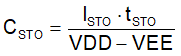
- ISTO is the internal STO current source, 400 mA.
- tSTO is the desired STO timing.
 Figure 9-13 Current Buffer
for Increased Drive Strength
Figure 9-13 Current Buffer
for Increased Drive Strength