SLUSDV7B October 2019 – March 2021 UCC23313-Q1
PRODUCTION DATA
- 1 Features
- 2 Applications
- 3 Description
- 4 Revision History
- 5 Pin Configuration and Function
-
6 Specifications
- 6.1 Absolute Maximum Ratings
- 6.2 ESD Ratings
- 6.3 Recommended Operating Conditions
- 6.4 Thermal Information
- 6.5 Power Ratings
- 6.6 Insulation Specifications
- 6.7 Safety-Related Certifications
- 6.8 Safety Limiting Values
- 6.9 Electrical Characteristics
- 6.10 Switching Characteristics
- 6.11 Insulation Characteristics Curves
- 6.12 Typical Characteristics
- 7 Parameter Measurement Information
- 8 Detailed Description
- 9 Application and Implementation
- 10Power Supply Recommendations
- 11Layout
- 12Mechanical, Packaging, and Orderable Information
Package Options
Refer to the PDF data sheet for device specific package drawings
Mechanical Data (Package|Pins)
- DWY|6
Thermal pad, mechanical data (Package|Pins)
Orderable Information
9.2.2.3 Estimate Gate-Driver Power Loss
The total loss, PG, in the gate-driver subsystem includes the power losses (PGD) of the UCC23313-Q1 device and the power losses in the peripheral circuitry, such as the external gate-drive resistor.
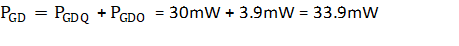
The PGD value is the key power loss which determines the thermal safety-related limits of the UCC23313-Q1 device, and it can be estimated by calculating losses from several components.
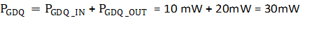
The first component is the static power loss, PGDQ, which includes power dissipated in the input stage (PGDQ_IN) as well as the quiescent power dissipated in the output stage (PGDQ_OUT) when operating with a certain switching frequency under no load. PGDQ_IN is determined by IF and VF and is given by Equation 5. The PGDQ_OUT parameter is measured on the bench with no load connected to VOUT pin at a given VCC, switching frequency, and ambient temperature. In this example, VCC is 15 V. The current on the power supply, with PWM switching at 10 kHz, is measured to be ICC = 1.33 mA . Therefore, use Equation 6 to calculate PGDQ_OUT.


The total quiescent power (without any load capacitance) dissipated in the gate driver is given by the sum of Equation 5 and Equation 6 as shown in Equation 7
The second component is the switching operation loss, PGDSW, with a given load capacitance which the driver charges and discharges the load during each switching cycle. Use Equation 8 to calculate the total dynamic loss from load switching, PGSW.

where
- QG is the gate charge of the power transistor at VCC.
So, for this example application the total dynamic loss from load switching is approximately 18 mW as calculated in Equation 9.

QG represents the total gate charge of the power transistor switching 520 V at 50 A, and is subject to change with different testing conditions. The UCC23313-Q1 gate-driver loss on the output stage, PGDO, is part of PGSW. PGDO is equal to PGSW if the external gate-driver resistance and power-transistor internal resistance are 0 Ω, and all the gate driver-loss will be dissipated inside the UCC23313-Q1. If an external turn-on and turn-off resistance exists, the total loss is distributed between the gate driver pull-up/down resistance, external gate resistance, and power-transistor internal resistance. Importantly, the pull-up/down resistance is a linear and fixed resistance if the source/sink current is not saturated to 4.5A/5.3A, however, it will be non-linear if the source/sink current is saturated. Therefore, PGDO is different in these two scenarios.
Case 1 - Linear Pull-Up/Down Resistor:

In this design example, all the predicted source and sink currents are less than 4.5 A and 5.3 A, therefore, use Equation 10 to estimate the UCC23313-Q1 gate-driver loss.

Case 2 - Nonlinear Pull-Up/Down Resistor:

where
- VOUT(t) is the gate-driver OUT pin voltage during the turnon and turnoff period. In cases where the output is saturated for some time, this value can be simplified as a constant-current source (4.5 A at turnon and 5.3 A at turnoff) charging or discharging a load capacitor. Then, the VOUT(t) waveform will be linear and the TR_Sys and TF_Sys can be easily predicted.
For some scenarios, if only one of the pullup or pulldown circuits is saturated and another one is not, the PGDO is a combination of case 1 and case 2, and the equations can be easily identified for the pullup and pulldown based on this discussion.
Use Equation 13 to calculate the total gate-driver loss dissipated in the UCC23313-Q1 gate driver, PGD.