SLUSDT9B May 2020 – March 2021 UCC23513-Q1
PRODUCTION DATA
- 1 Features
- 2 Applications
- 3 Description
- 4 Revision History
- 5 Pin Configuration and Function
-
6 Specifications
- 6.1 Absolute Maximum Ratings
- 6.2 ESD Ratings
- 6.3 Recommended Operating Conditions
- 6.4 Thermal Information
- 6.5 Power Ratings
- 6.6 Insulation Specifications
- 6.7 Safety-Related Certifications
- 6.8 Safety Limiting Values
- 6.9 Electrical Characteristics
- 6.10 Switching Characteristics
- 6.11 Insulation Characteristics Curves
- 6.12 Typical Characteristics
- 7 Parameter Measurement Information
- 8 Detailed Description
- 9 Application and Implementation
- 10Power Supply Recommendations
- 11Layout
- 12Mechanical, Packaging, and Orderable Information
Package Options
Mechanical Data (Package|Pins)
- DWY|6
Thermal pad, mechanical data (Package|Pins)
Orderable Information
3 Description
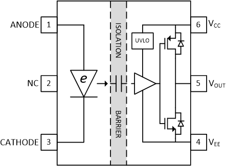
The UCC23513-Q1 driver are opto-compatible, single-channel, isolated gate drivers for IGBTs, MOSFETs and SiC MOSFETs, with 4.5-A source and 5.3-A sink peak output current and 5.7-kVRMS isolation rating. The high supply voltage range of 33-V allows the use of bipolar supplies to effectively drive IGBTs and SiC power FETs. UCC23513-Q1 can drive both low side and high side power FETs and bring significant performance and reliability upgrades over opto-coupler based gate drivers while maintaining pin-to-pin compatibility in both schematic and layout design. Performance highlights include high common mode transient immunity (CMTI), low propagation delay, and small pulse width distortion. Tight process control results in small part-to-part skew. The input stage is an emulated diode (e-diode) which means long term reliability and excellent aging characteristics compared to traditional LEDs found in optocoupler gate drivers. High performance and reliability makes them ideal for use in automotivemotor drives such as the traction inverter, on-board chargers, DC charging stations, and automotive HVAC and heating systems. The higher operating temperature opens up opportunities for applications not supported by traditional optocouplers.
| PART NUMBER | PACKAGE | BODY SIZE (NOM) |
|---|---|---|
| UCC23513-Q1 | Stretched SO-6 | 7.5 mm x 4.68 mm |
 Functional Block Diagram