SLUSD48C July 2018 – March 2022 UCC24624
PRODUCTION DATA
- 1 Features
- 2 Applications
- 3 Description
- 4 Revision History
- 5 Description, Continued
- 6 Pin Configuration and Functions
- 7 Specifications
- 8 Detailed Description
- 9 Application and Implementation
- 10Power Supply Recommendations
- 11Layout
- 12Device and Documentation Support
Package Options
Mechanical Data (Package|Pins)
- D|8
Thermal pad, mechanical data (Package|Pins)
Orderable Information
7.7 Typical Characteristics
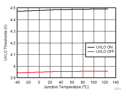 Figure 7-1 UVLO Thresholds vs Temperature
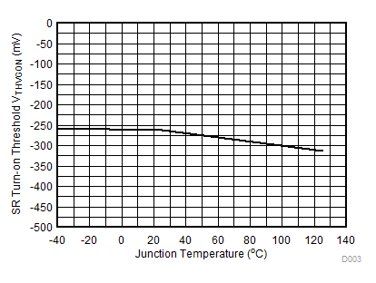 Figure 7-3 SR Turn-on Threshold Voltage vs Temperature
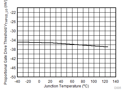 Figure 7-5 Proportional Gate Drive Threshold vs Temperature
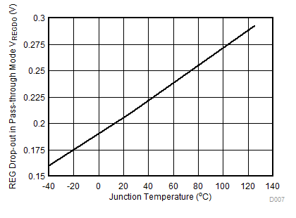
| ILOAD_REG = 10 mA |
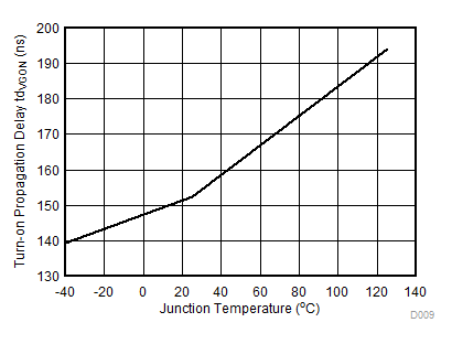 Figure 7-9 SR Turn-on Delay Time vs Temperature
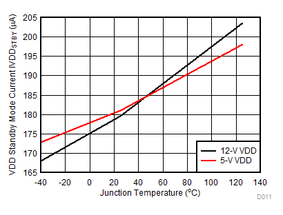 Figure 7-11 Standby Current vs Temperature
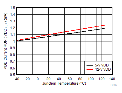
| CVG1 = CVG2 = 0 pF | VVD1= VVD2 = 1 V |
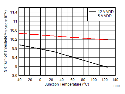 Figure 7-4 SR Turn-off Threshold Voltages vs Temperature
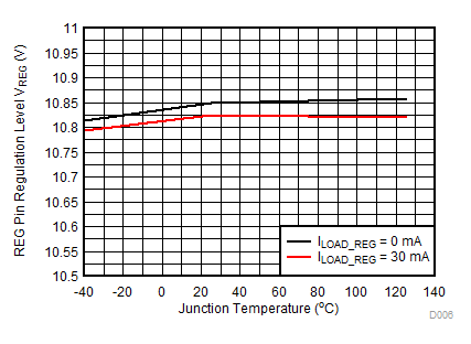 Figure 7-6 REG Pin Voltage vs Temperature at Different Loading Conditions
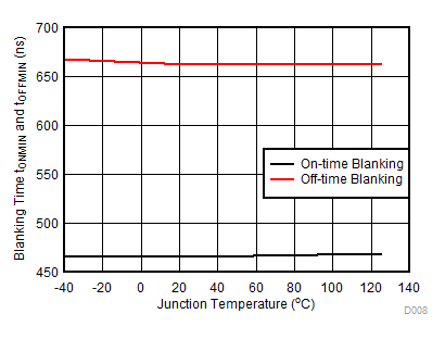 Figure 7-8 Blanking Time vs Temperature
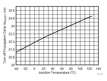 Figure 7-10 SR Turn-off Propagation Delay vs Temperature
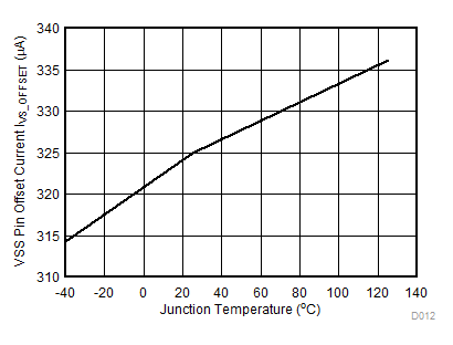 Figure 7-12 VSS Pin Offset Current vs Temperature