SLUSD48C July 2018 – March 2022 UCC24624
PRODUCTION DATA
- 1 Features
- 2 Applications
- 3 Description
- 4 Revision History
- 5 Description, Continued
- 6 Pin Configuration and Functions
- 7 Specifications
- 8 Detailed Description
- 9 Application and Implementation
- 10Power Supply Recommendations
- 11Layout
- 12Device and Documentation Support
Package Options
Mechanical Data (Package|Pins)
- D|8
Thermal pad, mechanical data (Package|Pins)
Orderable Information
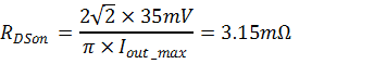
9.2.2.1 MOSFET Selection
In this UCC256302-based LLC resonant converter, the transformer secondary side is a center-tap structure. The SR MOSFET voltage stress, without considering the ringing voltages, must be twice of the output voltage. Given the 12-V output, this determines the SR steady state voltage stress of 24 V. However, due to the switching noises at MOSFET turn off, there is always extra voltage stress. To ensure enough design margin, 60-V rating MOSFETs were selected.
The selection of the MOSFET on-state resistance is the trade-off among performance at full load, light load, as well as cost. The lower on-state resistance gives lower conduction loss at heavy load while increases the switching loss at lighter load. It is also higher cost. Generally, the on-state resistance must be selected so that the 35-mV proportional gate drive threshold doesn't get activated until last 25% of the overall conduction time. The SR MOSFET on-state resistance can be selected as Equation 3. A 2.5-mΩ MOSFET was selected as the synchronous rectifier.