SLUSD48C July 2018 – March 2022 UCC24624
PRODUCTION DATA
- 1 Features
- 2 Applications
- 3 Description
- 4 Revision History
- 5 Description, Continued
- 6 Pin Configuration and Functions
- 7 Specifications
- 8 Detailed Description
- 9 Application and Implementation
- 10Power Supply Recommendations
- 11Layout
- 12Device and Documentation Support
Package Options
Mechanical Data (Package|Pins)
- D|8
Thermal pad, mechanical data (Package|Pins)
Orderable Information
3 Description
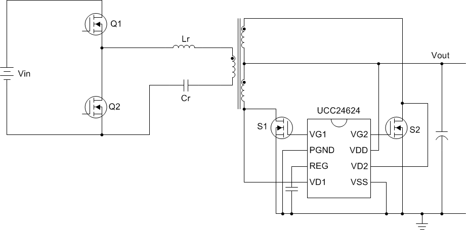
The UCC24624 high-performance synchronous rectifier (SR) controller is dedicated for LLC resonant converters to replace the lossy diode output rectifiers with SR MOSFETs and improve the overall system efficiency.
The UCC24624 SR controller uses drain-to-source voltage sensing method to achieve on and off control of the SR MOSFET. Proportional gate drive is implemented to extend the SR conduction time, minimize the body diode conduction time. To compensate for the offset voltage caused by the SR MOSFET parasitic inductance, the UCC24624 implements an adjustable positive turn-off threshold to accommodate different SR MOSFET packages. UCC24624 has a built-in 475-ns on-time blanking and a fixed 650-ns off-time blanking to avoid SR false turn-on and turn-off. UCC24624 also integrates a two-channel interlock function that prevents the two SRs from being on at the same time. With 230-V voltage-sensing pins and 28-V ABS maximum VDD rating, it can be directly used in converters with output voltage up to 24.75 V. The internal clamp allows the controller to support 36-V output voltage easily by adding an external current limiting resistor on VDD.
| PART NUMBER | PACKAGE | BODY SIZE (NOM) |
|---|---|---|
| UCC24624 | SOIC (8) | 4.90 mm × 3.91 mm |
 Typical Application
Schematic