SLUSCG2A March 2016 – March 2016 UCC24636
PRODUCTION DATA.
- 1 Features
- 2 Applications
- 3 Description
- 4 Revision History
- 5 Device Comparison Table
- 6 Pin Configuration and Functions
- 7 Specifications
- 8 Detailed Description
- 9 Application and Implementation
- 10Power Supply Recommendations
- 11Layout
- 12Device and Documentation Support
- 13Mechanical, Packaging, and Orderable Information
Package Options
Mechanical Data (Package|Pins)
- DBV|6
Thermal pad, mechanical data (Package|Pins)
Orderable Information
1 Features
- Secondary-Side SR Controller Optimized for 5-V to 24-V Output Discontinuous/Transition Mode Only Flyback Converters
- Volt-Second Balance Control Enables Highest Rectifier Efficiency
- Compatible with PSR and SSR Flyback Controllers
- Ultra Low 110-µA Standby Current Consumption
- Auto-Detect Standby Mode Disables SR Switching for Lower No-Load Power Consumption
- SR Turn-Off Independent of RDSON and Parasitic Inductance
- Operating Frequency Up to 130 kHz
- Wide VDD Range from 3.6 V to 28 V
- Adaptive Gate Drive Clamp
- Open and Short Pin Fault Protection
2 Applications
- AC/DC Adapters For Smartphones and Tablets
- USB Chargers with Type-C Connectors
- Notebook and Ultrabook Adapters
- High Efficiency Flyback Converters in Industrial SMPS
- High Efficiency Auxilliary Power In Server and Desktop Applications
3 Description
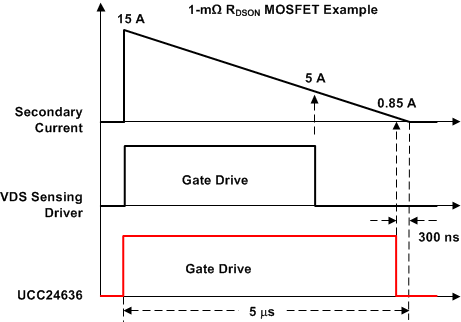
The UCC24636 SR is a compact, 6-pin secondary-side synchronous rectifier MOSFET controller and driver for high efficiency Flyback converters operating in Discontinuous (DCM) and Transition mode (TM). Unlike traditional SR controllers which measure the SR MOSFET drain voltage, UCC24636 implements a volt-second balance control method to determine the turn off transition of the SR MOSFET; hence, SR conduction time is independent of the MOSFET RDSON, parasitic inductance or ringing allowing flexibility to designers in component slelction and PCB layout. This control method enables maximum SR conduction time and highest rectifier efficiency for a given MOSFET.
The controller has built in intelligence to detect converter no load operation and automatically enters standby mode. While in standby mode, it disables the SR MOSFET and lowers its bias supply current to 110uA to further reduce overall system standby power consumption. The wide VDD operating range for the controller allows direct bias from the converter output for fixed or variable output voltage designs. This eliminates the need for an auxilliary winding on the main transformer, which simplifies the circuit design and reduces the cost.
Device Information(1)
| PART NUMBER | PACKAGE | BODY SIZE (NOM) |
|---|---|---|
| UCC24636 | SOT23 (6) | 2.92 mm x 1.30 mm |
- For all available packages, see the orderable addendum at the end of the data sheet.
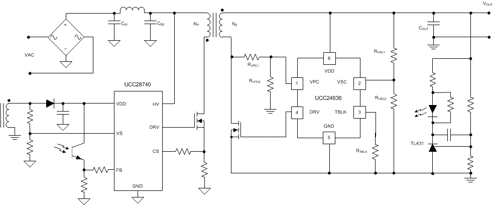
Simplified Schematic

Gate-Drive Timing vs VDS Sensing SR Driver
