SLUS846C September 2008 – June 2015 UCC25600
PRODUCTION DATA.
- 1 Features
- 2 Applications
- 3 Description
- 4 Revision History
- 5 Pin Configuration and Functions
- 6 Specifications
- 7 Detailed Description
- 8 Application and Implementation
- 9 Power Supply Recommendations
- 10Layout
- 11Device and Documentation Support
- 12Mechanical, Packaging, and Orderable Information
Package Options
Mechanical Data (Package|Pins)
- D|8
Thermal pad, mechanical data (Package|Pins)
Orderable Information
7 Detailed Description
7.1 Overview
Due to high power density and high efficiency requirements, LLC topology is employed in many applications. The LLC resonant converter has many unique characteristics and improvements compared with hard-switch bridge topology and phase-shift full bridge. For example, LLC has a simple structure, and could achieve primary MOSFET zero voltage switching (ZVS) and the secondary rectifier zero current switching (ZCS) from no load to full load.
The UCC25600 device is an LLC-resonant half-bridge controller which integrates built-in, state-of-the-art efficiency boost features with high-level protection features to provide cost-effective solutions.
7.2 Functional Block Diagram

7.3 Feature Description
7.3.1 Soft Start
During start-up and fault recovery conditions, soft start is always implemented to prevent excessive resonant tank current and to ensure zero-voltage switching (ZVS). During soft start, the switching frequency is increased. The soft-start time can be programmed by placing a capacitor from the SS pin to ground.
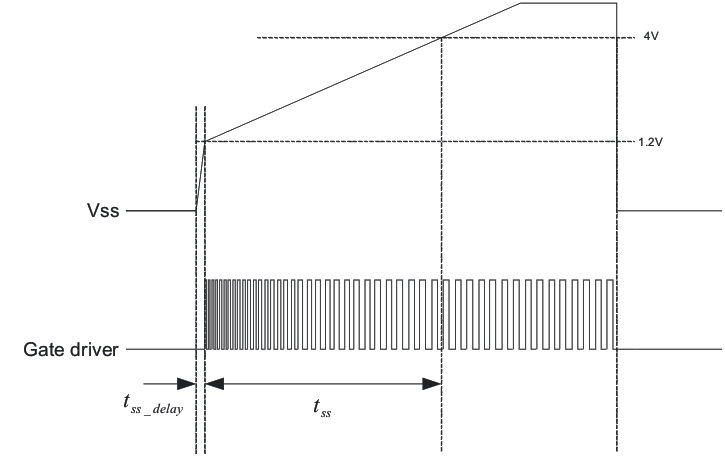
The soft-start pin also serves as an ON/OFF control pin of the device. By actively pulling the SS pin below 1 V, the device is disabled. When the pulldown is removed, SS pin voltage is increased because of internal charging current. Once the SS pin is above 1.2 V, the device starts to generate a gate-driver signal and enters soft-start mode. The time sequence of soft start is shown in Figure 12.
 Figure 12. Soft-Start Sequence
To prevent a long delay between the ON command and appearance of a gate driver signal, the SS pin current is set as two different levels. When the SS pin voltage is below 1.2 V, its output current is 175 μA. This high current could charge the soft-start pin capacitor to 1.2 V in a short period of time, and reduce the time delay. This time delay can be calculated using following equation:

The switching frequency during soft start is determined by both the current flowing out of the RT pin and the voltage on the SS pin. The switching frequency can be calculated based on the following equation:

After the SS pin voltage reaches 4 V, the soft-start period is finished and switching frequency becomes the same as demanded by the RT pin current. The time used to charge the SS pin from 1.2 V to 4 V is defined as soft-start time and can be calculated as:

To ensure reliable operation, the gate drivers restart with GD2 turning high. This prevents uncertainty during system start up.
7.3.2 Overcurrent Protection
To prevent power stage failure under excessive load current condition, the UCC25600 includes an overcurrent protection function. With a dedicated OC pin, the power stage is shut down when OC pin voltage is above 1 V. Once the OC pin voltage becomes lower than 0.6 V, the gate driver recovers with a soft start. To enhance system safety, the UCC25600 latches up the whole system when the OC pin becomes above 2 V. Bring VCC below the UVLO level to reset the device.
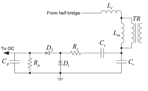
The current can be indirectly sensed through the voltage across the resonant capacitor by using the sensing network shown in Figure 13.
 Figure 13. Current Sensing for LLC Resonant Converter
The general concept of this sensing method is that the ac voltage across the resonant capacitor is proportional to load current.
According to the FHA model, peak voltage of the ac component on the resonant capacitor can be calculated as:

Therefore, the resonant capacitor voltage reaches its maximum value at the minimum switching frequency and maximum load. According to this equation, the current sensing network components can be calculated. Due to the nature of FHA, the final circuit parameters need to be verified through actual hardware test.
Table 2. Calculated Current Sensing Network Components
| NAME | FUNCTION | DESIGN EQUATION |
|---|---|---|
| RS | Transfer ac voltage across resonant capacitor into current source |
Equation 5.
 |
| CS | Blocking dc voltage on resonant capacitor |
Equation 6.
 |
| RP | Load resistor of the current source |
Equation 7.
 |
| CP | Filter capacitor |
Equation 8.
 |
7.3.3 Gate Driver
The half-bridge resonant converter is controlled by the nearly 50% duty-cycle variable frequency square-wave voltage. This allows the half bridge to be easily driven by the gate-driver transformer. Compared with a half-bridge driver device, a gate-driver transformer provides a simple and reliable solution, which:
- Eliminates the need for gate driver power supply
- Enables simplified layout
- Prevents shoot-through due to the transformer coupling
- Requires no latch up
The UCC25600 integrates two-gate drivers with 0.4-A source and 0.8-A sink capability to directly drive the gate-driver transformer.
For the LLC resonant converter, it is critical for the gate-driver signal to be precisely symmetrical. Otherwise, the resonant tank operation will be symmetrical. The load current distribution will be unbalanced for the output rectifiers, which in turn require the over-design of the power stages and thermal management.
In UCC25600, the gate-driver output is precisely trimmed to have less than 50-ns mismatch. Although the gate-driver signal is quite symmetrical, it is still recommended to insert the dc blocking capacitor in the gate-driver transformer primary side to prevent transformer saturation during fast transients.
7.3.4 Overtemperature Protection
UCC25600 continuously senses its junction temperature. When its junction temperature rises above 160°C, the device will enter overtemperature protection mode with both gate drivers actively pulled low. When junction temperature drops below 140°C, gate driver restarts with soft start.
7.4 Device Functional Modes
7.4.1 Burst-Mode Operation
During light load condition, the resonant converter tends to increase its switching frequency and maintain the output voltage regulation. However, due to ringing caused by the transformer parasitic capacitor and the rectification-diode-junction capacitors, the energy could be directly transferred to the load through these capacitors. When this power becomes more than the load requires, the output voltage become higher than the regulation level. In this case, further increasing the switching frequency will not help the situation because energy transfer to the load is not through the power stage itself.
To prevent output overvoltage during this condition, the UCC25600 includes the burst-mode operation function. When the control loop demands switching frequency higher than 350 kHz, the gate driver is disabled and the power stage stops switching. When the output voltage drops, the control loop begins to demand switching frequency less than 330 kHz, the gate driver recovers and the power stage begins to deliver power again. This allows the output voltage to be regulated.
This burst mode can be easily disabled by limiting the maximum switching frequency to less than 350 kHz. In this way, the control loop will never demand a switching frequency higher than 350 kHz and burst mode operation will not occur.
7.4.2 VCC
When VCC becomes above 10.5 V, the device is enabled and, after all fault conditions are cleared, the gate driver starts with soft start. When VCC drops below 9.5 V, the device enters the UVLO protection mode and both gate drivers are actively pulled low. When VCC rises above 20 V, the device enters VCC overvoltage protection mode and the device is disabled with both gate drivers actively pulled low. The VCC overvoltage protection will recover with soft start when the VCC voltage returns below 18 V.