SLUSCU6C August 2017 – January 2020 UCC256301
PRODUCTION DATA.
- 1 Features
- 2 Applications
- 3 Description
- 4 Revision History
- 5 Pin Configuration and Functions
- 6 Specifications
-
7 Detailed Description
- 7.1 Overview
- 7.2 Functional Block Diagram
- 7.3
Feature Description
- 7.3.1 Hybrid Hysteretic Control
- 7.3.2 Regulated 12-V Supply
- 7.3.3 Feedback Chain
- 7.3.4 Optocoupler Feedback Signal Input and Bias
- 7.3.5 System External Shut Down
- 7.3.6 Pick Lower Block and Soft Start Multiplexer
- 7.3.7 Pick Higher Block and Burst Mode Multiplexer
- 7.3.8 VCR Comparators
- 7.3.9 Resonant Capacitor Voltage Sensing
- 7.3.10 Resonant Current Sensing
- 7.3.11 Bulk Voltage Sensing
- 7.3.12 Output Voltage Sensing
- 7.3.13 High Voltage Gate Driver
- 7.3.14 Protections
- 7.4 Device Functional Modes
-
8 Application and Implementation
- 8.1 Application Information
- 8.2
Typical Application
- 8.2.1 Design Requirements
- 8.2.2
Detailed Design Procedure
- 8.2.2.1 LLC Power Stage Requirements
- 8.2.2.2 LLC Gain Range
- 8.2.2.3 Select Ln and Qe
- 8.2.2.4 Determine Equivalent Load Resistance
- 8.2.2.5 Determine Component Parameters for LLC Resonant Circuit
- 8.2.2.6 LLC Primary-Side Currents
- 8.2.2.7 LLC Secondary-Side Currents
- 8.2.2.8 LLC Transformer
- 8.2.2.9 LLC Resonant Inductor
- 8.2.2.10 LLC Resonant Capacitor
- 8.2.2.11 LLC Primary-Side MOSFETs
- 8.2.2.12 Design Considerations for Adaptive Dead-Time
- 8.2.2.13 LLC Rectifier Diodes
- 8.2.2.14 LLC Output Capacitors
- 8.2.2.15 HV Pin Series Resistors
- 8.2.2.16 BLK Pin Voltage Divider
- 8.2.2.17 BW Pin Voltage Divider
- 8.2.2.18 ISNS Pin Differentiator
- 8.2.2.19 VCR Pin Capacitor Divider
- 8.2.2.20 Burst Mode Programming
- 8.2.2.21 Soft-Start Capacitor
- 8.2.3 Application Curves
- 9 Power Supply Recommendations
- 10Layout
- 11Device and Documentation Support
- 12Mechanical, Packaging, and Orderable Information
Package Options
Mechanical Data (Package|Pins)
- DDB|14
Thermal pad, mechanical data (Package|Pins)
Orderable Information
7.4.3 X-Capacitor Discharge
X-capacitors used in EMC filters on the AC side of the diode bridge rectifier must have means to allow them to discharge to a reasonable voltage within certain time, this is to ensure that voltage does not remain present on the pins of the main cord indefinitely.
Typically explicit discharge resistors are provided in parallel with the capacitors to provide this discharge path, but these resistors then lead to fixed standing power loss as long as the power supply is connected to AC, and can be significant in the context of achieving very low standby power.
For every 100 nF of capacitance, a maximum bleed resistor of 10 MΩ must be added in parallel. For a typical 60-W to 100-W power supply with a typical capacitance of 330 nF, this requires 3 MΩ of discharge resistance. At nominal high line 230 V, these resistors dissipate 17.63 mW of standing power loss. Thus it is necessary to find alternative ways to discharge the X-capacitors using switched discharge paths, which avoid the static standing loss.
There are several standards about X-capacitor discharge. IEC60950 and IEC60065 requires that the discharge time constant is less than 1s; IEC62368 requires that after 2 seconds of AC unplug, the remaining voltage on the x-capacitor is less than 60 V (for 300 nF or more capacitance). UCC256301 uses an active discharge scheme to support the fast discharge of up to 5-μF X-capacitor.
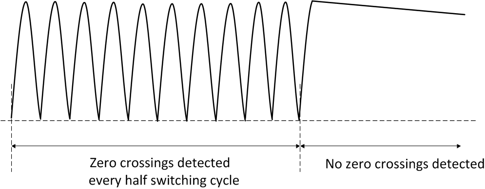
To meet the requirements of the standards, AC disconnect event should be detected. UCC256301 detects AC disconnect by monitoring the AC zero crossings through HV pin. When AC is present, there will be two AC zero crossings in one line cycle. When AC is disconnected, there will be no zero crossings for a long time. See Figure 44 shows the rectified AC waveform. In the figure, the AC is disconnected at the peak of the last half AC cycle. In reality, it can be disconnected anywhere in one switching cycle.
 Figure 44. AC Disconnect Waveform
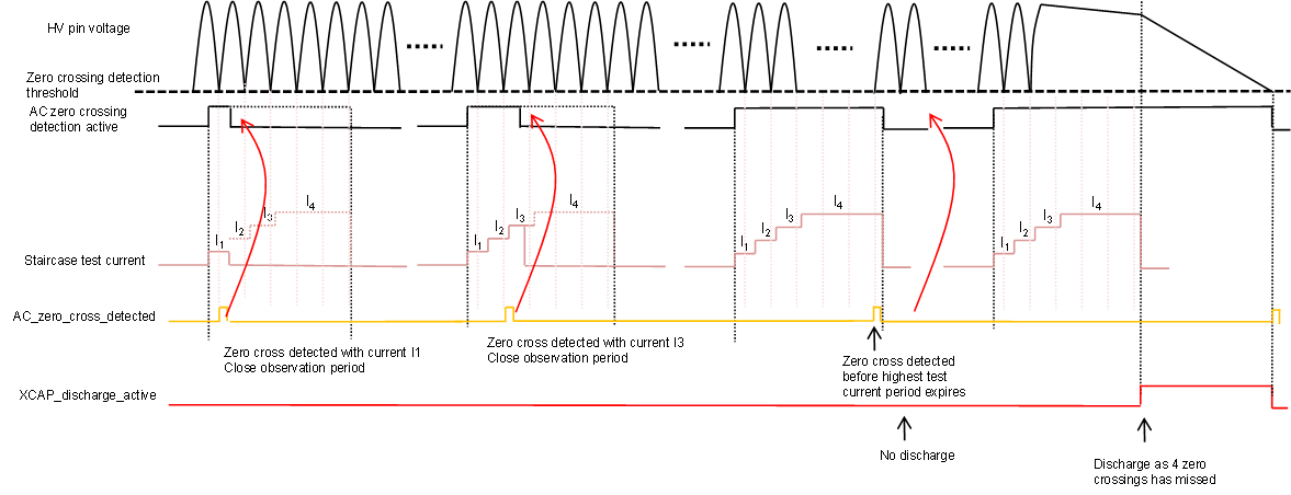
 To detect the zero crossings reliably as well as save power consumption, a stair case test current is generated every 700 ms. When there are 4 zero crossings missing in a row at the highest test current setting, AC disconnect is confirmed and the IXCapDischarge current source is enabled. The waveform below shows the stair case current waveform:
 Figure 45. Staircase Test Current for X-Capacitor Discharge
 The test current is required for reliable AC zero crossing sensing. In short, this is because the leakage current in the AC bridge rectifier diodes will affect zero crossing detection at very light load. The added test current on HV pin will overcome the leakage current and make sure that AC zero crossing is detected on HV pin. If one zero crossing is detected during any test current stage, it means that AC is not disconnected. The test current will shut off immediately and the system goes to the 700-ms no test current stage.
 Figure 46. Different Staircase Current Waveforms
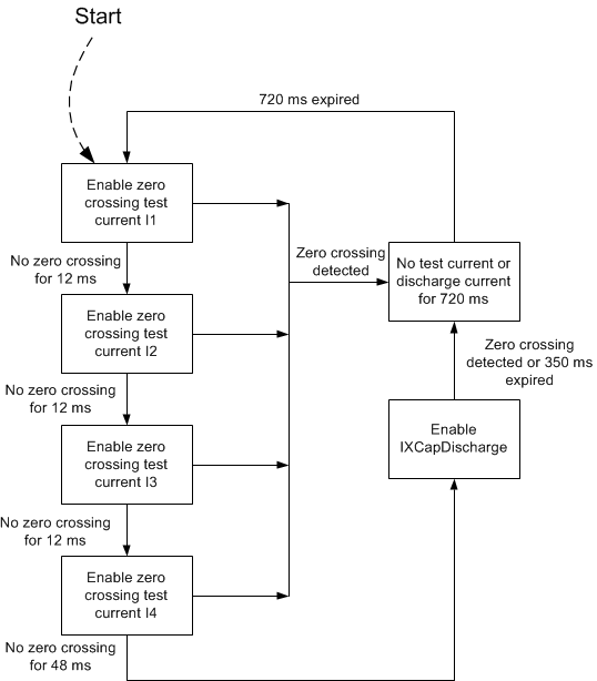
 Figure 46 shows different staircase current waveforms. The last waveform shows the AC disconnect is detected and x-cap discharge current is enabled. The x-cap discharge current is enabled until 350 ms has passed. AC zero crossing function is available in all operation modes and available all the time. Figure 47 shows the flow chart of AC zero crossing detection and X-capacitor discharge.
The discharge current IXCapDischarge is created by turning on the JFET and enable a current source from JFET source to GND. The reason to discharge to GND rather than discharge to VCC is to prevent VCC from reaching VCCStartSwitching. When AC is unplugged right before an OVP event, the voltage on the VCC is close to reaching VCCStartSwitching.
In LATCH state, the JFET is already on and acts as a pass element for the VCC regulation loop. The switch between the JFET source terminal and VCC pin is closed. If X-cap discharge current source is enabled without disconnect the JFET from the VCC pin, the discharge current has to discharge VCC voltage first, which requires a large amount of current to stay on for a long time. To avoid this issue, in LATCH state, the JFET is disconnected from VCC first. When the discharge phase is finished, turn the switch between JFET and VCC back on. Shown below is the circuit diagram and procedures of x-cap discharge in LATCH state.
 Figure 47. AC ZCD and X-capacitor Discharge Flow Chart