SLUSCU6C August 2017 – January 2020 UCC256301
PRODUCTION DATA.
- 1 Features
- 2 Applications
- 3 Description
- 4 Revision History
- 5 Pin Configuration and Functions
- 6 Specifications
-
7 Detailed Description
- 7.1 Overview
- 7.2 Functional Block Diagram
- 7.3
Feature Description
- 7.3.1 Hybrid Hysteretic Control
- 7.3.2 Regulated 12-V Supply
- 7.3.3 Feedback Chain
- 7.3.4 Optocoupler Feedback Signal Input and Bias
- 7.3.5 System External Shut Down
- 7.3.6 Pick Lower Block and Soft Start Multiplexer
- 7.3.7 Pick Higher Block and Burst Mode Multiplexer
- 7.3.8 VCR Comparators
- 7.3.9 Resonant Capacitor Voltage Sensing
- 7.3.10 Resonant Current Sensing
- 7.3.11 Bulk Voltage Sensing
- 7.3.12 Output Voltage Sensing
- 7.3.13 High Voltage Gate Driver
- 7.3.14 Protections
- 7.4 Device Functional Modes
-
8 Application and Implementation
- 8.1 Application Information
- 8.2
Typical Application
- 8.2.1 Design Requirements
- 8.2.2
Detailed Design Procedure
- 8.2.2.1 LLC Power Stage Requirements
- 8.2.2.2 LLC Gain Range
- 8.2.2.3 Select Ln and Qe
- 8.2.2.4 Determine Equivalent Load Resistance
- 8.2.2.5 Determine Component Parameters for LLC Resonant Circuit
- 8.2.2.6 LLC Primary-Side Currents
- 8.2.2.7 LLC Secondary-Side Currents
- 8.2.2.8 LLC Transformer
- 8.2.2.9 LLC Resonant Inductor
- 8.2.2.10 LLC Resonant Capacitor
- 8.2.2.11 LLC Primary-Side MOSFETs
- 8.2.2.12 Design Considerations for Adaptive Dead-Time
- 8.2.2.13 LLC Rectifier Diodes
- 8.2.2.14 LLC Output Capacitors
- 8.2.2.15 HV Pin Series Resistors
- 8.2.2.16 BLK Pin Voltage Divider
- 8.2.2.17 BW Pin Voltage Divider
- 8.2.2.18 ISNS Pin Differentiator
- 8.2.2.19 VCR Pin Capacitor Divider
- 8.2.2.20 Burst Mode Programming
- 8.2.2.21 Soft-Start Capacitor
- 8.2.3 Application Curves
- 9 Power Supply Recommendations
- 10Layout
- 11Device and Documentation Support
- 12Mechanical, Packaging, and Orderable Information
Package Options
Mechanical Data (Package|Pins)
- DDB|14
Thermal pad, mechanical data (Package|Pins)
Orderable Information
7.3.14.1 ZCS Region Prevention
Capacitive region is an LLC operation region in which the voltage gain increases when the switching frequency increases. It is also called ZCS region. Capacitive mode operation should be avoided for two reasons:
- The feedback loop becomes positive feedback in capacitive region
- The MOSFET may be damaged because of body diode reverse recovery
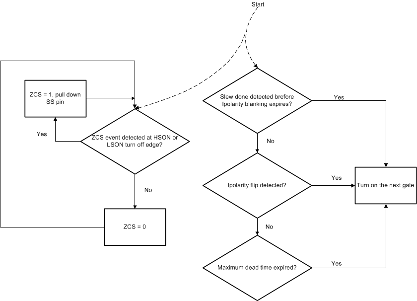
To make sure that capacitive region operation does not happen, we need to first rely on the slew done signal. If there is a slew done signal detected, it suggests that the opposite body diode must not be conducting and to turn on the next FET. If there is no slew detected, IPolarity signal is used. The next gate will be turned on at the next IPolarity flip event. The IPolarity flip indicates that the capacitive operation cycle has already passed. The resonant current reverses the direction and begins to discharge the switch node. When the capacitive operation cycle has passed, the system enters a high frequency oscillation stage, where the oscillation frequency is determined by the parasitic elements in the circuit. In this stage, the body diode is no longer conducting and it is allowed to turn on the next gate.
However, in the high frequency oscillation stage, the resonant current may be so small that the IPolarity detection is missed. In this case, the next gate will be turned on by maximum dead time timer expiration.
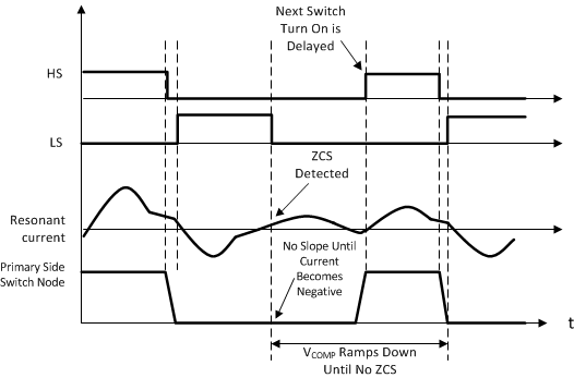
In addition to preventing the next gate from turning on when the opposite body diode is conducting, the switching frequency is forced to ramp up until there is a cycle with no capacitive region operation detected
The capacitive region detection is done by checking the resonant current polarity at HSON or LSON falling edge. If the resonant current is positive at LSON falling edge, or negative at HSON falling edge, the ZCS signal in the waveform generator is turned high. The ZCS signal keeps high until there is a half cycle without capacitive region operation happens.
The force ramping up of the switching frequency is done by pull the SS pin down by a resistor to ground. Details will be discussed in SS pin section.
Below is the flow chart of capacitive region prevention algorithm:
 Figure 41. Gate Driver Block Diagram
  Figure 42. Timing Diagram of a ZCS Event