SLUSD49A September 2017 – January 2019 UCC256303
PRODUCTION DATA.
- 1 Features
- 2 Applications
- 3 Description
- 4 Revision History
- 5 Pin Configuration and Functions
- 6 Specifications
-
7 Detailed Description
- 7.1 Overview
- 7.2 Functional Block Diagram
- 7.3
Feature Description
- 7.3.1 Hybrid Hysteretic Control
- 7.3.2 Regulated 12-V Supply
- 7.3.3 Feedback Chain
- 7.3.4 Optocoupler Feedback Signal Input and Bias
- 7.3.5 System External Shut Down
- 7.3.6 Pick Lower Block and Soft Start Multiplexer
- 7.3.7 Pick Higher Block and Burst Mode Multiplexer
- 7.3.8 VCR Comparators
- 7.3.9 Resonant Capacitor Voltage Sensing
- 7.3.10 Resonant Current Sensing
- 7.3.11 Bulk Voltage Sensing
- 7.3.12 Output Voltage Sensing
- 7.3.13 High Voltage Gate Driver
- 7.3.14 Protections
- 7.4 Device Functional Modes
-
8 Application and Implementation
- 8.1 Application Information
- 8.2
Typical Application
- 8.2.1 Design Requirements
- 8.2.2
Detailed Design Procedure
- 8.2.2.1 LLC Power Stage Requirements
- 8.2.2.2 LLC Gain Range
- 8.2.2.3 Select Ln and Qe
- 8.2.2.4 Determine Equivalent Load Resistance
- 8.2.2.5 Determine Component Parameters for LLC Resonant Circuit
- 8.2.2.6 LLC Primary-Side Currents
- 8.2.2.7 LLC Secondary-Side Currents
- 8.2.2.8 LLC Transformer
- 8.2.2.9 LLC Resonant Inductor
- 8.2.2.10 LLC Resonant Capacitor
- 8.2.2.11 LLC Primary-Side MOSFETs
- 8.2.2.12 Design Considerations for Adaptive Dead-Time
- 8.2.2.13 LLC Rectifier Diodes
- 8.2.2.14 LLC Output Capacitors
- 8.2.2.15 BLK Pin Voltage Divider
- 8.2.2.16 BW Pin Voltage Divider
- 8.2.2.17 ISNS Pin Differentiator
- 8.2.2.18 VCR Pin Capacitor Divider
- 8.2.2.19 Burst Mode Programming
- 8.2.2.20 Soft-Start Capacitor
- 8.2.3 Application Curves
- 9 Power Supply Recommendations
- 10Layout
- 11Device and Documentation Support
- 12Mechanical, Packaging, and Orderable Information
Package Options
Refer to the PDF data sheet for device specific package drawings
Mechanical Data (Package|Pins)
- DDB|14
Thermal pad, mechanical data (Package|Pins)
Orderable Information
7.4.1 Burst Mode Control
The efficiency of an LLC converter power stage drops rapidly with falling output power. To maintain reasonable light load efficiency it is necessary to operate the LLC converter in burst mode. In this mode the LLC converter operates at relatively high power for a short burst period and then all switching is stopped for a space period. During the Burst period excess charge is transferred to and stored in the output capacitor. During the Space period this stored charge is used to supply the load current. Providing an effective light-load scheme is a particular problem for an LLC controller that is located on the primary side of the isolation barrier. This is because the feedback demand signal (VCOMP) is mainly a function of input/output voltage ratio and only loosely related to load current. The normal method of placing a couple of thresholds in the VCOMP voltage window to switch OFF and ON the LLC converter does not work effectively. Another issue with the conventional method is that when burst on, the switching pulses are determined by VCOMP, which is usually at initial burst on, and decays as the output voltage rises. The resulting inductor current will be big at first and then decays. This is not optimal because the big current at first may create mechanical vibration. The high switching frequency afterwards may cause two much switching loss.
For an advanced burst mode, the following features are desired:
- The power delivered by each burst should be relatively constant for a certain load.
- The Burst power is set high enough to provide reasonable LLC converter efficiency and low enough to avoid acoustic noise and excessive output voltage ripple.
- When burst on, the average capacitor voltage should settle to VIN/2 as fast as possible for best efficiency.
- The switching frequency or burst power level of each burst pulse should be optimized for efficient operation.
- The burst pattern of each burst should be relatively constant.
- There should be no audible noise.
- Burst mode performance should be consistent across input voltage range.
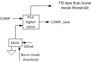
The HHC method makes the control of the burst mode very straight forward. The block diagram is a functionally accurate description of the burst mode control method in UCC256303.
 Figure 36. Burst Mode Control Block Diagram
 The control effort is selected between the higher of the two signals: 1) the voltage loop compensator output (VCOMP) or 2) the Burst Mode Threshold level (BMT). When VCOMP goes below BMT, continue switching for a fixed number of switching cycles, then stop. Always switch while COMP is higher than BMT. If soft start isn’t done yet, send the COMP (controlled by soft start ramp). BMT is programmable and adaptively changed with input voltage. The last pulse of each burst on period is turned off when the resonant capacitor voltage equals VIN/2. In HHC method, this is approximately equivalent to VCR node voltage equals the common mode voltage VCM. This operation keeps the resonant capacitor voltage to about VIN/2 for each burst off period, thus enabling the burst pattern to settle as soon as possible during burst on period.