SLUSD49A September 2017 – January 2019 UCC256303
PRODUCTION DATA.
- 1 Features
- 2 Applications
- 3 Description
- 4 Revision History
- 5 Pin Configuration and Functions
- 6 Specifications
-
7 Detailed Description
- 7.1 Overview
- 7.2 Functional Block Diagram
- 7.3
Feature Description
- 7.3.1 Hybrid Hysteretic Control
- 7.3.2 Regulated 12-V Supply
- 7.3.3 Feedback Chain
- 7.3.4 Optocoupler Feedback Signal Input and Bias
- 7.3.5 System External Shut Down
- 7.3.6 Pick Lower Block and Soft Start Multiplexer
- 7.3.7 Pick Higher Block and Burst Mode Multiplexer
- 7.3.8 VCR Comparators
- 7.3.9 Resonant Capacitor Voltage Sensing
- 7.3.10 Resonant Current Sensing
- 7.3.11 Bulk Voltage Sensing
- 7.3.12 Output Voltage Sensing
- 7.3.13 High Voltage Gate Driver
- 7.3.14 Protections
- 7.4 Device Functional Modes
-
8 Application and Implementation
- 8.1 Application Information
- 8.2
Typical Application
- 8.2.1 Design Requirements
- 8.2.2
Detailed Design Procedure
- 8.2.2.1 LLC Power Stage Requirements
- 8.2.2.2 LLC Gain Range
- 8.2.2.3 Select Ln and Qe
- 8.2.2.4 Determine Equivalent Load Resistance
- 8.2.2.5 Determine Component Parameters for LLC Resonant Circuit
- 8.2.2.6 LLC Primary-Side Currents
- 8.2.2.7 LLC Secondary-Side Currents
- 8.2.2.8 LLC Transformer
- 8.2.2.9 LLC Resonant Inductor
- 8.2.2.10 LLC Resonant Capacitor
- 8.2.2.11 LLC Primary-Side MOSFETs
- 8.2.2.12 Design Considerations for Adaptive Dead-Time
- 8.2.2.13 LLC Rectifier Diodes
- 8.2.2.14 LLC Output Capacitors
- 8.2.2.15 BLK Pin Voltage Divider
- 8.2.2.16 BW Pin Voltage Divider
- 8.2.2.17 ISNS Pin Differentiator
- 8.2.2.18 VCR Pin Capacitor Divider
- 8.2.2.19 Burst Mode Programming
- 8.2.2.20 Soft-Start Capacitor
- 8.2.3 Application Curves
- 9 Power Supply Recommendations
- 10Layout
- 11Device and Documentation Support
- 12Mechanical, Packaging, and Orderable Information
Package Options
Refer to the PDF data sheet for device specific package drawings
Mechanical Data (Package|Pins)
- DDB|14
Thermal pad, mechanical data (Package|Pins)
Orderable Information
7.3.10 Resonant Current Sensing
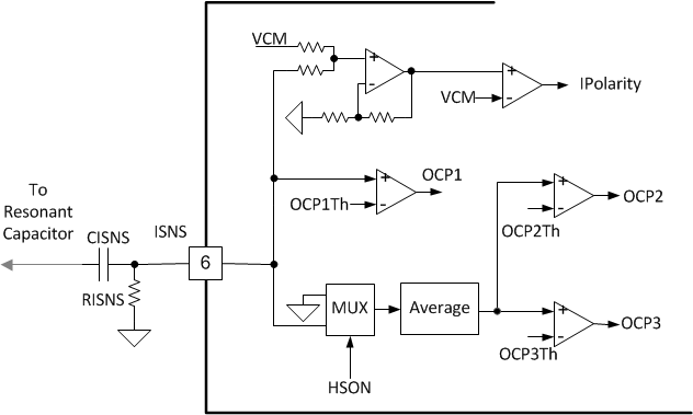
The ISNS pin is connected to the resonant capacitor using a high voltage capacitor. The capacitor CISNS and the resistor RISNS form a differentiator. The resonant capacitor voltage is differentiated to get the resonant current. The differentiated signal is AC and goes both positive and negative. In order to sense the zero crossing, the signal is level shifted using an op amp adder. IPolarity comparator detects the direction of the resonant current. The digital state machine implements a blanking time on IPolarity – IPolarity edges during the first 400ns of dead time are ignored.
OCP2 and OCP3 thresholds are based on average input current. To get the average input current, the differentiator output is multiplexed with the high side switch on signal HSON: when HS is on, the MUX output is the differentiator output; when HS is off, the MUX output is 0. The MUX output is then averaged using a low pass filter. The output of the filter is the sensed average input current. Note that the MUX needs to pass through both positive and negative voltages. OCP2 and OCP3 faults have a 2ms and 50ms timer respectively. Only when the OCP2/OCP3 comparators output high for continuous 2ms or 50ms, the faults will be activated.
OCP1 threshold is set on the peak resonant current. The voltage on the ISNS pin gets compared to OCP1 threshold OCP1Th directly. The peak resonant current is checked once per cycle on the positive half cycle. OCP1 fault is only activated when there are 4 consecutive cycles of OCP1 event detected. During start up, the OCP1 comparator output of the first 15 cycles are ignored.
 Figure 28. ISNS Block Diagram