SLUSD90E June   2019  – February 2021 UCC256402 , UCC256403 , UCC256404

PRODUCTION DATA  

  1. Features
  2. Applications
  3. Description
  4. Revision History
    1.     Device Comparison Table
  5. Pin Configuration and Functions
    1.     Pin Functions
  6. Specifications
    1. 6.1 Absolute Maximum Ratings
    2. 6.2 ESD Ratings
    3. 6.3 Recommended Operating Conditions
    4. 6.4 Thermal Information
    5. 6.5 Electrical Characteristics
    6. 6.6 Switching Characteristics
    7. 6.7 Typical Characteristics
  7. Detailed Description
    1. 7.1 Overview
    2. 7.2 Functional Block Diagram
    3. 7.3 Feature Description
      1. 7.3.1 Hybrid Hysteretic Control
      2. 7.3.2 Regulated 13-V Supply
      3. 7.3.3 Feedback Chain
        1. 7.3.3.1 Optocoupler Feedback Signal Input and Bias
        2. 7.3.3.2 FB Pin Voltage Clamp
        3. 7.3.3.3 "Pick Lower Value" Block and Soft Start Multiplexer
        4. 7.3.3.4 Pick Higher Block and Burst Mode Multiplexer
        5. 7.3.3.5 VCR Comparators
      4. 7.3.4 Resonant Capacitor Voltage Sensing
      5. 7.3.5 Resonant Current Sensing
      6. 7.3.6 Bulk Voltage Sensing
      7. 7.3.7 Output Voltage Sensing
      8. 7.3.8 High Voltage Gate Driver
        1. 7.3.8.1 Adaptive Dead Time Control
      9. 7.3.9 Protections
        1. 7.3.9.1 ZCS Region Prevention
        2. 7.3.9.2 Over Current Protection (OCP)
        3. 7.3.9.3 Bias Winding Over Voltage Protection (BWOVP)
        4. 7.3.9.4 Input Under Voltage Protection (VINUVP)
        5. 7.3.9.5 Input Over Voltage Protection (VINOVP)
        6. 7.3.9.6 Boot UVLO
        7. 7.3.9.7 RVCC UVLO
        8. 7.3.9.8 Over Temperature Protection (OTP)
    4. 7.4 Device Functional Modes
      1. 7.4.1 High Voltage Start-Up
      2. 7.4.2 X-Capacitor Discharge
      3. 7.4.3 Burst Mode Control
        1. 7.4.3.1 Soft-Start and Burst-Mode Threshold
        2. 7.4.3.2 BMTL/BMTH Ratio Programming
      4. 7.4.4 System State Machine
  8. Power Supply Recommendations
    1. 8.1 VCC Pin Capacitor
    2. 8.2 Boot Capacitor
    3. 8.3 RVCC Pin Capacitor
  9. Layout
    1. 9.1 Layout Guidelines
    2. 9.2 Layout Example
  10. 10Device and Documentation Support
    1. 10.1 Documentation Support
      1. 10.1.1 Related Documentation
    2. 10.2 Related Links
    3. 10.3 Receiving Notification of Documentation Updates
    4. 10.4 Community Resources
    5. 10.5 Trademarks

Package Options

Mechanical Data (Package|Pins)
Thermal pad, mechanical data (Package|Pins)
Orderable Information

VCC Pin Capacitor

The VCC capacitor should be sized based on the total start-up charge required by the system. The start-up charge will mostly be consumed by the gate driver circuit. Thus the total start-up charge can be estimated by the start-up switching frequency, MOSFET gate charge, and the soft-start time.

Assume the total start-up charge required by the system is shown in Equation 80

Equation 80. GUID-63BDB053-C1B2-4A71-87FD-550F273BDE3D-low.gif

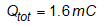
During PFC and LLC startup phase, the maximum VCC voltage drop allowed is

Equation 81. GUID-E04C0251-A464-48F7-8EA2-52FCDA4F309C-low.gif

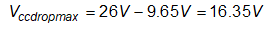
The minimum VCC capacitor needed:

Equation 82. GUID-80A600B4-77E8-4F9D-818E-5385B543FDC2-low.gif

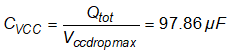
Choose at least 100 µF capacitor or combination of capacitors.