SLUSD90E June 2019 – February 2021 UCC256402 , UCC256403 , UCC256404
PRODUCTION DATA
- 1 Features
- 2 Applications
- 3 Description
- 4 Revision History
- 5 Pin Configuration and Functions
- 6 Specifications
-
7 Detailed Description
- 7.1 Overview
- 7.2 Functional Block Diagram
- 7.3 Feature Description
- 7.4 Device Functional Modes
- 8 Power Supply Recommendations
- 9 Layout
- 10Device and Documentation Support
Package Options
Mechanical Data (Package|Pins)
- DDB|14
Thermal pad, mechanical data (Package|Pins)
Orderable Information
7.3.4 Resonant Capacitor Voltage Sensing
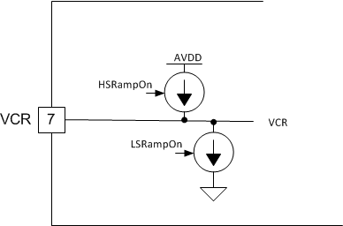
The resonant capacitor voltage sense pin senses the resonant capacitor voltage through a capacitor divider. Inside the device, two well matched, controlled current sources are connected to the VCR pin to generate the frequency compensation ramp. The on/off control signals of the two current sources come from the waveform generator block.
During waveform generator IDLE state or before startup, the VCR node is clamped to VCM. This action will help reduce the startup peak current, and help the VCR voltage to settle down quickly during burst mode.
 Figure 7-5 VCR Block Diagram
The ramp current on/off sequence is shown in Figure 7-6. The ramp current is on all the time. It changes direction at the falling edge of the high-side on or low-side on signal.
 Figure 7-6 VCR Compensation Ramp Current On/Off
On the VCR pin, a capacitor divider is used to combine the resonant capacitor waveform and the compensation ramp waveform. Adjusting the size of the external capacitors can change the contribution of charge control and direct frequency control. Assuming the divided down version of the resonant capacitor voltage by the capacitor divider is Vdiv, the compensation ramp current resultant voltage on the VCR pin is Vramp. If Vdiv is much larger than Vramp, the control method is similar to charge control, in which the control effort is proportional to the input charge of one switching cycle. If Vramp is much larger than Vdiv, the control method is similar to direct frequency control, in which the control effort is proportional to the switching frequency. The most optimal transient response can be achieved by adjusting the ratio between Vdiv and Vramp.