SLUSD90E June   2019  – February 2021 UCC256402 , UCC256403 , UCC256404

PRODUCTION DATA  

  1. Features
  2. Applications
  3. Description
  4. Revision History
    1.     Device Comparison Table
  5. Pin Configuration and Functions
    1.     Pin Functions
  6. Specifications
    1. 6.1 Absolute Maximum Ratings
    2. 6.2 ESD Ratings
    3. 6.3 Recommended Operating Conditions
    4. 6.4 Thermal Information
    5. 6.5 Electrical Characteristics
    6. 6.6 Switching Characteristics
    7. 6.7 Typical Characteristics
  7. Detailed Description
    1. 7.1 Overview
    2. 7.2 Functional Block Diagram
    3. 7.3 Feature Description
      1. 7.3.1 Hybrid Hysteretic Control
      2. 7.3.2 Regulated 13-V Supply
      3. 7.3.3 Feedback Chain
        1. 7.3.3.1 Optocoupler Feedback Signal Input and Bias
        2. 7.3.3.2 FB Pin Voltage Clamp
        3. 7.3.3.3 "Pick Lower Value" Block and Soft Start Multiplexer
        4. 7.3.3.4 Pick Higher Block and Burst Mode Multiplexer
        5. 7.3.3.5 VCR Comparators
      4. 7.3.4 Resonant Capacitor Voltage Sensing
      5. 7.3.5 Resonant Current Sensing
      6. 7.3.6 Bulk Voltage Sensing
      7. 7.3.7 Output Voltage Sensing
      8. 7.3.8 High Voltage Gate Driver
        1. 7.3.8.1 Adaptive Dead Time Control
      9. 7.3.9 Protections
        1. 7.3.9.1 ZCS Region Prevention
        2. 7.3.9.2 Over Current Protection (OCP)
        3. 7.3.9.3 Bias Winding Over Voltage Protection (BWOVP)
        4. 7.3.9.4 Input Under Voltage Protection (VINUVP)
        5. 7.3.9.5 Input Over Voltage Protection (VINOVP)
        6. 7.3.9.6 Boot UVLO
        7. 7.3.9.7 RVCC UVLO
        8. 7.3.9.8 Over Temperature Protection (OTP)
    4. 7.4 Device Functional Modes
      1. 7.4.1 High Voltage Start-Up
      2. 7.4.2 X-Capacitor Discharge
      3. 7.4.3 Burst Mode Control
        1. 7.4.3.1 Soft-Start and Burst-Mode Threshold
        2. 7.4.3.2 BMTL/BMTH Ratio Programming
      4. 7.4.4 System State Machine
  8. Power Supply Recommendations
    1. 8.1 VCC Pin Capacitor
    2. 8.2 Boot Capacitor
    3. 8.3 RVCC Pin Capacitor
  9. Layout
    1. 9.1 Layout Guidelines
    2. 9.2 Layout Example
  10. 10Device and Documentation Support
    1. 10.1 Documentation Support
      1. 10.1.1 Related Documentation
    2. 10.2 Related Links
    3. 10.3 Receiving Notification of Documentation Updates
    4. 10.4 Community Resources
    5. 10.5 Trademarks

Package Options

Mechanical Data (Package|Pins)
Thermal pad, mechanical data (Package|Pins)
Orderable Information
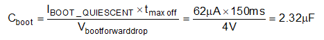
Boot Capacitor

During burst off period, power consumed by the high-side gate driver from the HB pin must be drawn from CBOOT and will cause its voltage to decay. At the start of the next burst period there must be sufficient voltage remaining on CBOOT to power the high-side gate driver until the conduction period of LO allows it to be replenished from CRVCC. The power consumed by the high-side driver during this burst off period will therefore have a direct impact on the size and cost of capacitors that must be connected to HB and RVCC.

Assume the system has a maximum burst off period of 150 ms and the bootstrap diode has a forward voltage drop of 1V. Target a minimum bootstrap voltage of 8 V to avoid UVLO fault. The maximum allowable voltage drop on the boot capacitor is:

Equation 83. GUID-A143F46B-0180-4B02-9D2B-5EC39FCC3F0B-low.gif

Boot capacitor can then be sized:

Equation 84. GUID-70D98754-5EDB-40E4-988E-04B54E76C052-low.gif