SLUSD90E June 2019 – February 2021 UCC256402 , UCC256403 , UCC256404
PRODUCTION DATA
- 1 Features
- 2 Applications
- 3 Description
- 4 Revision History
- 5 Pin Configuration and Functions
- 6 Specifications
-
7 Detailed Description
- 7.1 Overview
- 7.2 Functional Block Diagram
- 7.3 Feature Description
- 7.4 Device Functional Modes
- 8 Power Supply Recommendations
- 9 Layout
- 10Device and Documentation Support
Package Options
Mechanical Data (Package|Pins)
- DDB|14
Thermal pad, mechanical data (Package|Pins)
Orderable Information
7.4.2 X-Capacitor Discharge
X-capacitors used in EMC filters on the AC side of the diode bridge rectifier must have a method to allow them to discharge down to a reasonable voltage within a specific amount of time. This is to ensure that voltage does not remain present on the pins of the AC plug indefinitely after it is physically removed from the AC power.
Typically, discharge resistors are provided in parallel with the X-capacitors to provide this discharge path, but these resistors then lead to fixed standing power loss as long as the power supply is connected to AC power, and can be significant in the context of achieving very low standby power.
For every 100 nF of capacitance, a maximum bleed resistor of 10 MΩ must be added in parallel. For a typical 60-W to 100-W power supply with a typical capacitance of 330 nF, this requires 3 MΩ of discharge resistance. At nominal high line 230 V, these resistors dissipate 17.63 mW of standing power loss. Thus it is necessary to find alternative ways to discharge the X-capacitors using switched discharge paths in order to avoid the static standing loss.
There are several standards for X-capacitor discharge. IEC60950 and IEC60065 requires that the discharge time constant is less than 1s. IEC62368 requires that after 2 seconds of AC unplug, the remaining voltage on the x-capacitor is less than 60 V (for 300 nF or more capacitance). UCC25640x uses an active discharge scheme to support the fast discharge of up to 5-μF X-capacitance, for device variants that has X-capacitor discharge.
To meet the requirements of the standards, AC disconnect events must be detected. UCC25640x detects AC disconnect by monitoring the AC zero crossings through the HV pin. When AC is present, there will be two AC zero crossings in one line cycle. When AC is disconnected, there will be no zero crossings for an extended period of time. Figure 7-13 shows the rectified AC waveform. In the figure, the AC is disconnected at the peak of the last half AC cycle. In reality, it can be disconnected anywhere within a switching cycle.
 Figure 7-13 AC Disconnect Waveform
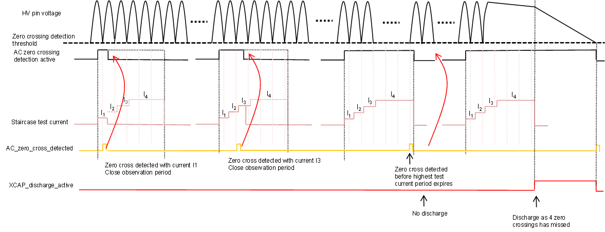
To detect the zero crossings reliably as well as save power consumption, a staircase test current is generated every 700 ms. When there are 4 zero crossings missing in a row at the highest test current setting, AC disconnect is confirmed and the IXCapDischarge current source is enabled. The waveform below shows the staircase current waveform:
 Figure 7-14 Staircase Test Current for X-Capacitor Discharge
The test current is required for reliable AC zero crossing sensing. In short, this is because the leakage current in the AC bridge rectifier diodes will affect the zero crossing detection at very light load. The added test current on the HV pin will overcome the leakage current and make sure that AC zero crossing is detected on the HV pin. If one zero crossing is detected during any test current stage, it means that AC is not disconnected. The test current will shut off immediately and the system goes to the 700-ms no test current stage.
 Figure 7-15 Different Staircase Current Waveforms
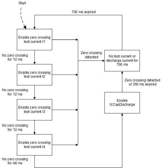
Figure 7-15 shows different staircase current waveforms. The last waveform shows the AC disconnect is detected and X-capacitor discharge current is enabled. The X-capacitor discharge current is enabled for 350 ms. AC zero crossing function is available in all operation modes and available all the time. Figure 7-16 shows the flow chart of AC zero crossing detection and X-capacitor discharge. The zero crossing test starts 12 ms after HV startup is completed. The discharge current IXCapDischarge is created by turning on the JFET and enabling a current source from JFET source to GND. During a fault restart process, HV startup is higher priority, so that the JFET is connected to VCC. A zero crossing test current will be sent out 12 ms after HV startup is completed, regardless of whether the detection idle timer has expired.
In some of the device variants, the X-capacitor discharge feature is disabled.
 Figure 7-16 AC ZCD and X-Capacitor Discharge Flow Chart