SLUS746C December 2006 – April 2016 UCC27200 , UCC27201
PRODUCTION DATA.
- 1 Features
- 2 Applications
- 3 Description
- 4 Revision History
- 5 Pin Configuration and Functions
- 6 Specifications
- 7 Detailed Description
- 8 Application and Implementation
- 9 Power Supply Recommendations
- 10Layout
- 11Device and Documentation Support
- 12Mechanical, Packaging, and Orderable Information
Package Options
Mechanical Data (Package|Pins)
Thermal pad, mechanical data (Package|Pins)
- DDA|8
Orderable Information
6 Specifications
6.1 Absolute Maximum Ratings
over operating free-air temperature, unless noted, all voltages are with respect to VSS.(1)| MIN | MAX | UNIT | ||
|---|---|---|---|---|
| Supply voltage, VDD(2) | –0.3 | 20 | V | |
| Input voltages on LI and HI, VLI, VHI | –0.3 | 20 | V | |
| Output voltage on LO, VLO | DC | –0.3 | VDD + 0.3 | V |
| Repetitive pulse < 100 ns(3) | –2 | VDD + 0.3 | ||
| Output voltage on HO, VHO | DC | VHS – 0.3 | VHB + 0.3 | V |
| Repetitive pulse < 100 ns(3) | VHS – 2 | VHB + 0.3 | ||
| Voltage on HS, VHS | DC | –1 | 120 | V |
| Repetitive pulse < 100 ns(3) | –5 | 120 | ||
| Voltage on HB, VHB | –0.3 | 120 | V | |
| Voltage on HB-HS | –0.3 | 20 | V | |
| Power dissipation at TA = 25°C | (D package)(4) | 1.3 | W | |
| (DDA package)(4) | 2.7 | |||
| (DRM package)(4) | 3.3 | |||
| Lead temperature (soldering, 10 s) | 300 | °C | ||
| Operating virtual junction temperature, TJ | –40 | 150 | °C | |
| Storage temperature, Tstg | –65 | 150 | °C | |
(1) Stresses beyond those listed under Absolute Maximum Ratings may cause permanent damage to the device. These are stress ratings only, which do not imply functional operation of the device at these or any other conditions beyond those indicated under Recommended Operating Conditions. Exposure to absolute-maximum-rated conditions for extended periods may affect device reliability.
(2) All voltages are with respect to Vss. Currents are positive into, negative out of the specified terminal.
(3) Values are verified by characterization and are not production tested.
(4) This data was taken using the JEDEC proposed high-K test PCB. See Thermal Information for details.
6.2 ESD Ratings
| VALUE | UNIT | |||
|---|---|---|---|---|
| V(ESD) | Electrostatic discharge | Human-body model (HBM), per ANSI/ESDA/JEDEC JS-001(1) | ±2000 | V |
| Charged-device model (CDM), per JEDEC specification JESD22-C101(2) | ±1000 | |||
(1) JEDEC document JEP155 states that 500-V HBM allows safe manufacturing with a standard ESD control process.
(2) JEDEC document JEP157 states that 250-V CDM allows safe manufacturing with a standard ESD control process.
6.3 Recommended Operating Conditions
over operating free-air temperature range (unless otherwise noted)| MIN | NOM | MAX | UNIT | |||
|---|---|---|---|---|---|---|
| VDD | Supply voltage | 8 | 12 | 17 | V | |
| VHS | Voltage on HS | –1 | 105 | V | ||
| repetitive pulse < 100 ns | –5 | 110 | ||||
| VHB | Voltage on HB | VHS + 8 | 115 | V | ||
| Voltage slew rate on HS | 50 | V/ns | ||||
| TJ | Operating junction temperature | –40 | 140 | °C | ||
6.4 Thermal Information
PDISS = (150 – TA) / θJA, unless otherwise noted.| THERMAL METRIC(1) | UCC27200, UCC27201 | UNIT | |||
|---|---|---|---|---|---|
| D (SOIC) | DDA (HSOP) | DRM (VSON) | |||
| 8 PINS | 8 PINS | 8 PINS | |||
| RθJA | Junction-to-ambient thermal resistance | 106.5 | 40.5 | 36.2 | °C/W |
| RθJC(top) | Junction-to-case (top) thermal resistance | 52.9 | 49 | 41.6 | °C/W |
| RθJB | Junction-to-board thermal resistance | 46.6 | 10.2 | 13.2 | °C/W |
| ψJT | Junction-to-top characterization parameter | 9.6 | 3.1 | 0.6 | °C/W |
| ψJB | Junction-to-board characterization parameter | 46.1 | 9.7 | 13.4 | °C/W |
| RθJC(bot) | Junction-to-case (bottom) thermal resistance | — | 1.5 | 3.1 | °C/W |
(1) For more information about traditional and new thermal metrics, see the Semiconductor and IC Package Thermal Metrics application report, SPRA953.
6.5 Electrical Characteristics
over operating free-air temperature range, VDD = VHB = 12 V, VHS = VSS = 0 V, No load on LO or HO, TA = TJ = –40°C to 140°C, (unless otherwise noted)| PARAMETER | TEST CONDITIONS | MIN | TYP | MAX | UNIT | ||
|---|---|---|---|---|---|---|---|
| SUPPLY CURRENTS | |||||||
| IDD | VDD quiescent current | VLI = VHI = 0 | 0.4 | 0.8 | mA | ||
| IDDO | VDD operating current | f = 500 kHz, CLOAD = 0 | UCC27200 | 2.5 | 4 | ||
| UCC27201 | 3.8 | 5.5 | |||||
| IHB | Boot voltage quiescent current | VLI = VHI = 0 V | 0.4 | 0.8 | |||
| IHBO | Boot voltage operating current | f = 500 kHz, CLOAD = 0 | 2.5 | 4 | |||
| IHBS | HB to VSS quiescent current | VHS = VHB = 110 V | 0.0005 | 1 | uA | ||
| IHBSO | HB to VSS operating current | f = 500 kHz, CLOAD = 0 | 0.1 | mA | |||
| INPUT | |||||||
| VHIT | Input rising threshold | UCC27200 | 5.8 | 8 | V | ||
| VLIT | Input falling threshold | 3 | 5.4 | ||||
| VIHYS | Input voltage hysteresis | 0.4 | |||||
| VHIT | Input voltage threshold | UCC27201 | 1.7 | 2.5 | |||
| VLIT | Input voltage threshold | 0.8 | 1.6 | ||||
| VIHYS | Input voltage Hysteresis | 100 | mV | ||||
| RIN | Input pulldown resistance | 100 | 200 | 350 | kΩ | ||
| UNDERVOLTAGE PROTECTION (UVLO) | |||||||
| VDD rising threshold | 6.2 | 7.1 | 7.8 | V | |||
| VDD threshold hysteresis | 0.5 | ||||||
| VHB rising threshold | 5.8 | 6.7 | 7.2 | ||||
| VHB threshold hysteresis | 0.4 | ||||||
| BOOTSTRAP DIODE | |||||||
| VF | Low-current forward voltage | I VDD – HB = 100 μA | 0.65 | 0.85 | V | ||
| VFI | High-current forward voltage | I VDD – HB = 100 mA | 0.85 | 1.1 | |||
| RD | Dynamic resistance, ΔVF / ΔI | I VDD – HB = 100 mA and 80 mA | 0.6 | 1 | Ω | ||
| LO GATE DRIVER | |||||||
| VLOL | Low-level output voltage | ILO = 100 mA | 0.18 | 0.4 | V | ||
| VLOH | High-level output voltage | ILO = –100 mA, VLOH = VDD – VLO |
TJ = –40 to 125°C | 0.25 | 0.4 | ||
| TJ = –40 to 140°C | 0.25 | 0.42 | |||||
| Peak pullup current | VLO = 0 V | 3 | A | ||||
| Peak pulldown current | VLO = 12 V | 3 | |||||
| HO GATE DRIVER | |||||||
| VHOL | Low-level output voltage | IHO = 100 mA | 0.18 | 0.4 | V | ||
| VHOH | High-level output voltage | IHO = –100 mA, VHOH = VHB – VHO |
TJ = –40 to 125°C | 0.25 | 0.4 | ||
| TJ = –40 to 140°C | 0.25 | 0.42 | |||||
| Peak pullup current | VHO = 0 V | 3 | A | ||||
| Peak pulldown current | VHO = 12 V | 3 | |||||
| PROPAGATION DELAYS | |||||||
| TDLFF | VLI falling to VLO falling | CLOAD = 0 | TJ = –40 to 125°C | 20 | 45 | ns | |
| TJ = –40 to 140°C | 20 | 50 | |||||
| TDHFF | VHI falling to VHO falling | CLOAD = 0 | TJ = –40 to 125°C | 20 | 45 | ||
| TJ = –40 to 140°C | 20 | 50 | |||||
| TDLRR | VLI rising to VLO rising | CLOAD = 0 | TJ = –40 to 125°C | 20 | 45 | ||
| TJ = –40 to 140°C | 20 | 50 | |||||
| TDHRR | VHI rising to VHO rising | CLOAD = 0 | TJ = –40 to 125°C | 20 | 45 | ||
| TJ = –40 to 140°C | 20 | 50 | |||||
| DELAY MATCHING | |||||||
| TMON | LI ON, HI OFF | 1 | 7 | ns | |||
| TMOFF | LI OFF, HI ON | 1 | 7 | ||||
| OUTPUT RISE AND FALL TIME | |||||||
| tR | LO, HO | CLOAD = 1000 pF | 8 | ns | |||
| tF | LO, HO | CLOAD = 1000 pF | 7 | ||||
| tR | LO, HO (3 V to 9 V) | CLOAD = 0.1 μF | 0.35 | 0.6 | us | ||
| tF | LO, HO (3 V to 9 V) | CLOAD = 0.1 μF | 0.3 | 0.6 | |||
| MISCELLANEOUS | |||||||
| Minimum input pulse width that changes the output | 50 | ns | |||||
| Bootstrap diode turn-off time | IF = 20 mA, IREV = 0.5 A(1)(2) | 20 | |||||
(1) Typical values for TA = 25°C
(2) IF: Forward current applied to bootstrap diode, IREV: Reverse current applied to bootstrap diode.
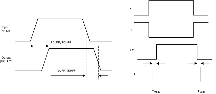 Figure 1. Timing Diagrams
6.6 Typical Characteristics
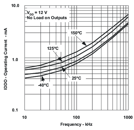 Figure 2. UCC27200 IDD Operating Current vs Frequency
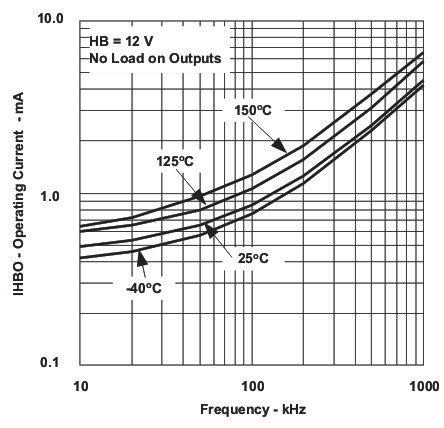 Figure 4. Boot Voltage Operating Current vs Frequency
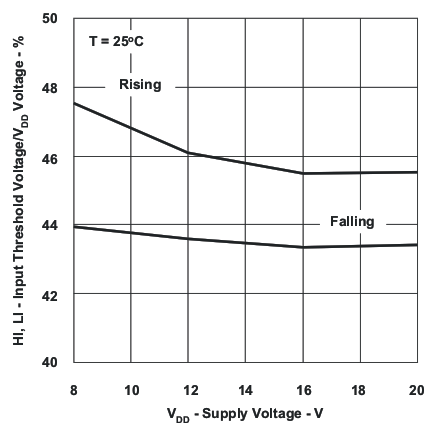 Figure 6. UCC27200 Input Threshold vs Supply Voltage
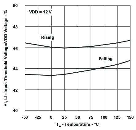 Figure 8. UCC27200 Input Threshold vs Temperature
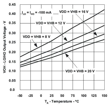 Figure 10. LO and HO High-Level Output Voltage vs Temperature
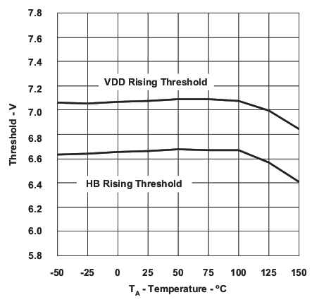 Figure 12. Undervoltage Lockout Threshold vs Temperature
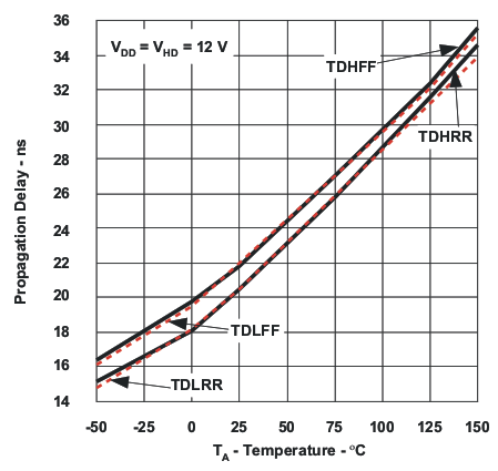 Figure 14. UCC27200 Propagation Delays vs Temperature
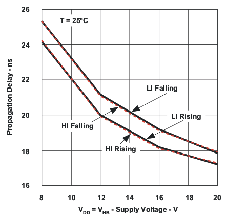 Figure 16. UCC27200 Propagation Delay vs Supply Voltage
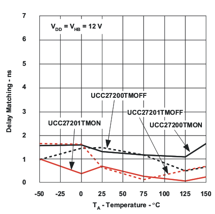 Figure 18. Delay Matching vs Temperature
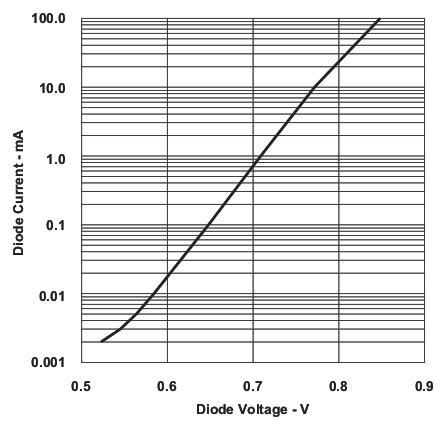 Figure 20. Diode Current vs Diode Voltage
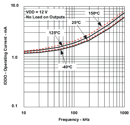 Figure 3. UCC27201 IDD Operating Current vs Frequency
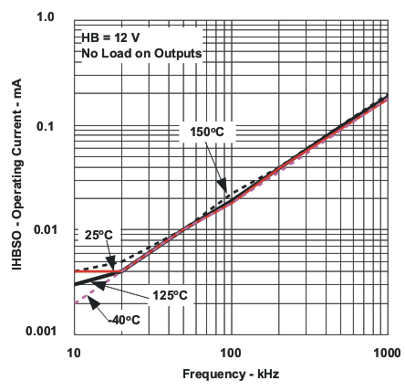 Figure 5. HB to VSS Operating Current vs Frequency
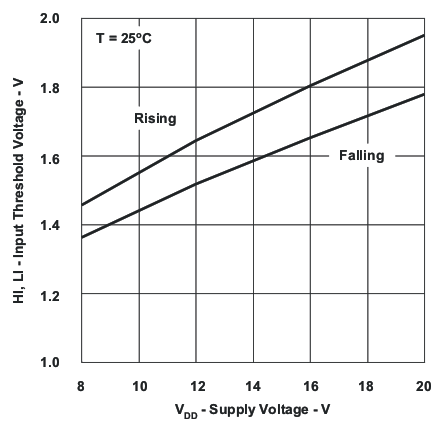 Figure 7. UCC27201 Input Threshold vs Supply Voltage
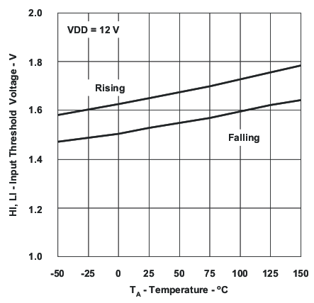 Figure 9. UCC27201 Input Threshold vs Temperature
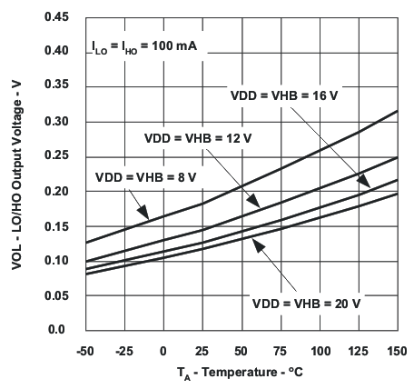 Figure 11. LO and HO Low-Level Output Voltage vs Temperature
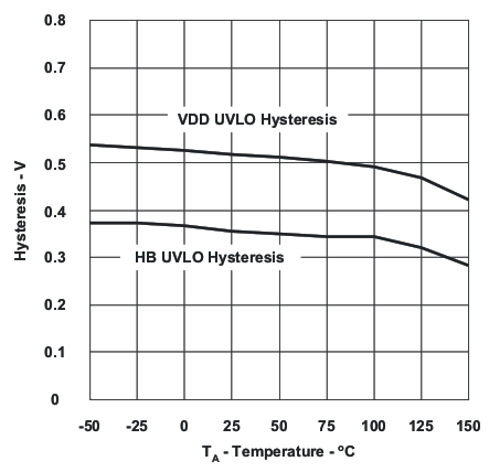 Figure 13. Undervoltage Lockout Threshold Hysteresis vs Temperature
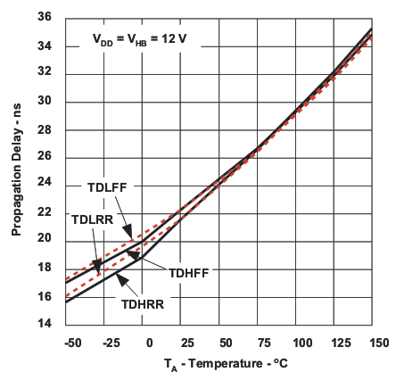 Figure 15. UCC27201 Propagation Delays vs Temperature
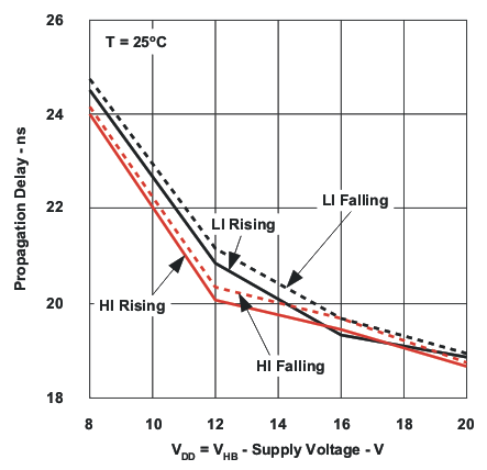 Figure 17. UCC27201 Propagation Delay vs Supply Voltage
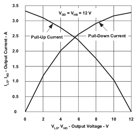 Figure 19. Output Current vs Output Voltage
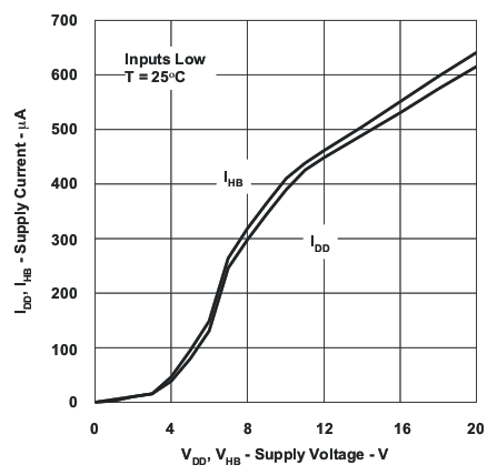 Figure 21. Quiescent Current vs Supply Voltage