SLUSC72B May 2015 – March 2016 UCC27201A-Q1
PRODUCTION DATA.
- 1 Features
- 2 Applications
- 3 Description
- 4 Revision History
- 5 Pin Configuration and Functions
- 6 Specifications
- 7 Detailed Description
- 8 Application and Implementation
- 9 Power Supply Recommendations
- 10Layout
- 11Device and Documentation Support
- 12Mechanical, Packaging, and Orderable Information
Package Options
Mechanical Data (Package|Pins)
Thermal pad, mechanical data (Package|Pins)
- DDA|8
Orderable Information
7 Detailed Description
7.1 Overview
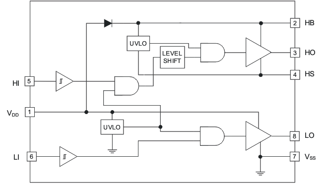
The UCC27201A-Q1 is a high-side/low-side driver. The high-side and low-side each have independent inputs which allow maximum flexibility of input control signals in the application. The boot diode for the high-side driver bias supply is internal to the UCC27201A-Q1. The UCC27201-Q1 inputs are TTL-compatible. The high-side driver is referenced to the switch node (HS) which is typically the source pin of the high side MOSFET and drain pin of the low-side MOSFET. The low-side driver is referenced to VSS which is typically ground. The functions contained are the input stages, UVLO protection, level shift, boot diode, and output driver stages.
7.2 Functional Block Diagram

7.3 Feature Description
7.3.1 Input Stages
The input stages provide the interface to the PWM output signals. The input stages of the UCC27201A-Q1 incorporate an open drain configuration to provide the lower input thresholds. The input impedance is 200 kΩ nominal and input capacitance is approximately 4 pF. The 200 kΩ is a pull-down resistance to VSS (ground). The logic level compatible input provides a rising threshold of 1.7 V and a falling threshold of 1.6 V.
7.3.1.1 UVLO (Under Voltage Lockout)
The bias supplies for the high-side and low-side drivers have UVLO protection. VDD as well as VHB to VHS differential voltages are monitored. The VDD UVLO disables both drivers when VDD is below the specified threshold. The rising VDD threshold is 7.1 V with 0.5-V hysteresis. The VHB UVLO disables only the high-side driver when the VHB to VHS differential voltage is below the specified threshold. The VHB UVLO rising threshold is 6.7 V with 0.4-V hysteresis.
7.3.1.2 Level Shift
The level shift circuit is the interface from the high-side input to the high-side driver stage which is referenced to the switch node (HS). The level shift allows control of the HO output referenced to the HS pin and provides excellent delay matching with the low-side driver.
7.3.1.3 Boot Diode
The boot diode necessary to generate the high-side bias is included in the UCC27201A-Q1 driver. The diode anode is connected to VDD and cathode connected to VHB. With the VHB capacitor connected to HB and the HS pins, the VHB capacitor charge is refreshed every switching cycle when HS transitions to ground. The boot diode provides fast recovery times, low diode resistance, and voltage rating margin to allow for efficient and reliable operation.
7.3.1.4 Output Stages
The output stages are the interface to the power MOSFETs in the power train. High slew rate, low resistance and high peak current capability of both output drivers allow for efficient switching of the power MOSFETs. The low-side output stage is referenced from VDD to VSS and the high-side is referenced from VHB to VHS.
7.4 Device Functional Modes
The device operates in normal mode and UVLO mode. See UVLO (Under Voltage Lockout) for more information on UVLO operation mode. In normal mode, the output stage is dependent on the states of the HI and LI pins.