SLUSCG0A December   2015  – January 2016 UCC27211A-Q1

PRODUCTION DATA.  

  1. Features
  2. Applications
  3. Description
    1.     Device Images
      1.      Typical Application Diagram
      2.      Propagation Delays vs Supply Voltage T = 25°C
  4. Revision History
  5. Description (continued)
  6. Pin Configuration and Functions
    1.     Pin Functions
  7. Specifications
    1. 7.1 Absolute Maximum Ratings
    2. 7.2 ESD Ratings
    3. 7.3 Recommended Operating Conditions
    4. 7.4 Thermal Information
    5. 7.5 Electrical Characteristics
    6. 7.6 Switching Characteristics
    7. 7.7 Typical Characteristics
  8. Detailed Description
    1. 8.1 Overview
    2. 8.2 Functional Block Diagram
    3. 8.3 Feature Description
      1. 8.3.1 Input Stages
      2. 8.3.2 Undervoltage Lockout (UVLO)
      3. 8.3.3 Level Shift
      4. 8.3.4 Boot Diode
      5. 8.3.5 Output Stages
    4. 8.4 Device Functional Modes
  9. Application and Implementation
    1. 9.1 Application Information
    2. 9.2 Typical Application
      1. 9.2.1 Design Requirements
      2. 9.2.2 Detailed Design Procedure
        1. 9.2.2.1 Input Threshold Type
        2. 9.2.2.2 VDD Bias Supply Voltage
        3. 9.2.2.3 Peak Source and Sink Currents
        4. 9.2.2.4 Propagation Delay
        5. 9.2.2.5 Power Dissipation
      3. 9.2.3 Application Curves
  10. 10Power Supply Recommendations
  11. 11Layout
    1. 11.1 Layout Guidelines
    2. 11.2 Layout Example
    3. 11.3 Thermal Considerations
  12. 12Device and Documentation Support
    1. 12.1 Documentation Support
      1. 12.1.1 Related Documentation
    2. 12.2 Community Resources
    3. 12.3 Trademarks
    4. 12.4 Electrostatic Discharge Caution
    5. 12.5 Glossary
  13. 13Mechanical, Packaging, and Orderable Information

Package Options

Mechanical Data (Package|Pins)
Thermal pad, mechanical data (Package|Pins)
Orderable Information

Typical Characteristics

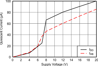
UCC27211A-Q1 0001_IDD_IHB_vs_VDD_VHB_lusat7.gif
T = 25°C
Figure 2. Quiescent Current vs Supply Voltage
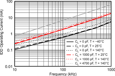
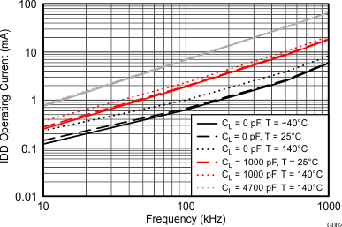
UCC27211A-Q1 0003_UCC27211_IDDO_vs_Freq_lusat7.gif
VDD = 12 V
Figure 4. IDD Operating Current vs Frequency
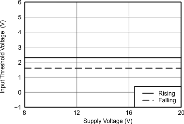
UCC27211A-Q1 0005_VIHL_vs_VDD_lusat7.gif
T = 25°C
Figure 6. Input Threshold vs Supply Voltage
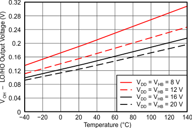
UCC27211A-Q1 0007_VOH_vs_Temp_lusat7.gif
IHO = ILO = 100 mA
Figure 8. LO and HO High-Level Output Voltage
vs Temperature
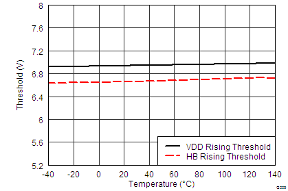
UCC27211A-Q1 0009_UVLO_vs_Temp_lusat7.png
Figure 10. Undervoltage Lockout Threshold
vs Temperature
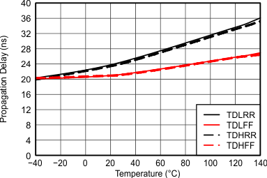
UCC27211A-Q1 0011_UCC27210_Delay_vs_Temp_lusat7.gif
VDD = VHB = 12 V
Figure 12. Propagation Delays vs Temperature
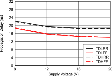
UCC27211A-Q1 0014_UCC27211_Delay_vs_VDD_lusat7.gif
T = 25°C
Figure 14. Propagation Delays vs Supply Voltage
(VDD = VHB)
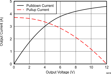
UCC27211A-Q1 out_new_sluscg0.gif
VDD = VHB = 12 V
Figure 16. Output Current vs Output Voltage
UCC27211A-Q1 0002_UCC27210_IDDO_vs_Freq_lusat7.gif
VDD = 12 V
Figure 3. IDD Operating Current vs Frequency
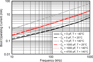
UCC27211A-Q1 0004_IHBO_vs_Freq_lusat7.gif
VHB – VHS = 12 V
Figure 5. Boot Voltage Operating Current vs
Frequency (HB To HS)
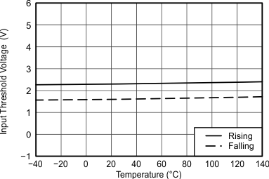
UCC27211A-Q1 0006_VIHL_vs_Temp_lusat7.gif
VDD = 12 V
Figure 7. Input Thresholds vs Temperature
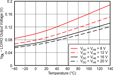
UCC27211A-Q1 0008_VOL_vs_Temp_lusat7.gif
IHO = ILO = 100 mA
Figure 9. LO and HO Low-Level Output Voltage
vs Temperature
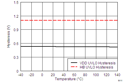
UCC27211A-Q1 0010_UVLO_HYS_vs_Temp_lusat7.png
Figure 11. Undervoltage Lockout Threshold Hysteresis
vs Temperature
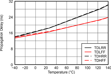
UCC27211A-Q1 0012_UCC27211_Delay_vs_Temp_lusat7.gif
VDD = VHB = 12 V
Figure 13. Propagation Delays vs Temperature
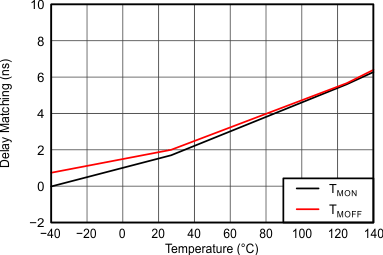
UCC27211A-Q1 0015_DelayMatching_vs_Temp_lusat7.gif
VDD = VHB = 12 V
Figure 15. Delay Matching vs Temperature
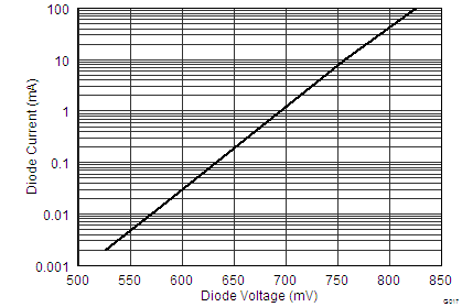
UCC27211A-Q1 0017_DiodeCurrent_vs_DiodeVoltage_lusat7.png
Figure 17. Diode Current vs Diode Voltage