SLUSBL4C August 2013 – October 2015 UCC27211A
PRODUCTION DATA.
- 1 Features
- 2 Applications
- 3 Description
- 4 Revision History
- 5 Description (continued)
- 6 Pin Configuration and Functions
-
7 Specifications
- 7.1 Absolute Maximum Ratings
- 7.2 ESD Ratings
- 7.3 Recommended Operating Conditions
- 7.4 Thermal Information
- 7.5 Electrical Characteristics
- 7.6 Switching Characteristics: Propagation Delays
- 7.7 Switching Characteristics: Delay Matching
- 7.8 Switching Characteristics: Output Rise and Fall Time
- 7.9 Switching Characteristics: Miscellaneous
- 7.10 Typical Characteristics
- 8 Detailed Description
- 9 Application and Implementation
- 10Power Supply Recommendations
- 11Layout
- 12Device and Documentation Support
- 13Mechanical, Packaging, and Orderable Information
Package Options
Mechanical Data (Package|Pins)
- DRM|8
Thermal pad, mechanical data (Package|Pins)
- DRM|8
Orderable Information
11 Layout
11.1 Layout Guidelines
To improve the switching characteristics and efficiency of a design, the following layout rules must be followed.
- Locate the driver as close as possible to the MOSFETs.
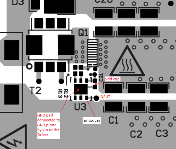
- Locate the VDD – VSS and VHB-VHS (bootstrap) capacitors as close as possible to the device (see Figure 23).
- Pay close attention to the GND trace. Use the thermal pad of the DRM package as GND by connecting it to the VSS pin (GND). The GND trace from the driver goes directly to the source of the MOSFET, but must not be in the high current path of the MOSFET drain or source current.
- Use similar rules for the HS node as for GND for the high-side driver.
- For systems using multiple and UCC27211A devices, TI recommends that dedicated decoupling capacitors be located at VDD-VSS for each device.
- Care must be taken to avoid placing VDD traces close to LO, HS, and HO signals.
- Use wide traces for LO and HO closely following the associated GND or HS traces. A width of 60 to 100 mils is preferable where possible.
- Use as least two or more vias if the driver outputs or SW node must be routed from one layer to another. For GND, the number of vias must be a consideration of the thermal pad requirements as well as parasitic inductance.
- Avoid LI and HI (driver input) going close to the HS node or any other high dV/dT traces that can induce significant noise into the relatively high impedance leads.
A poor layout can cause a significant drop in efficiency or system malfunction, and it can even lead to decreased reliability of the whole system.
11.2 Layout Example
 Figure 23. UCC27211A PCB Layout Example
11.3 Thermal Considerations
The useful range of a driver is greatly affected by the drive-power requirements of the load and the thermal characteristics of the package. For a gate driver to be useful over a particular temperature range, the package must allow for efficient removal of the heat produced while keeping the junction temperature within rated limits. The thermal metrics for the driver package are listed in Thermal Information. For detailed information regarding the table, refer to the Application Note from Texas Instruments entitled Semiconductor and IC Package Thermal Metrics (SPRA953). The UCC27211A device is offered in SOIC (8) and VSON (8). The Thermal Information section lists the thermal performance metrics related to the SOT-23 package.