SNVSAQ5B November 2018 – May 2022 UCC27282
PRODUCTION DATA
- 1 Features
- 2 Applications
- 3 Description
- 4 Revision History
- 5 Pin Configuration and Functions
- 6 Specifications
- 7 Detailed Description
- 8 Application and Implementation
- 9 Power Supply Recommendations
- 10Layout
- 11Device and Documentation Support
- 12Mechanical, Packaging, and Orderable Information
Package Options
Mechanical Data (Package|Pins)
Thermal pad, mechanical data (Package|Pins)
- DRC|10
Orderable Information
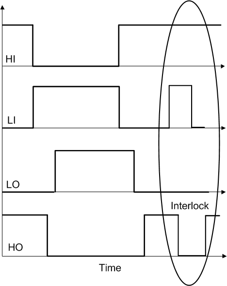
7.3.3 Input Stages and Interlock
The two inputs operate independently, with an exception that both outputs will be pulled low when both inputs are high or overlap. The independence allows for full control of two outputs compared to the gate drivers that have a single input. The device has input interlock or cross-conduction protection. Whenever both the inputs are high, the internal logic turns both the outputs off. Once the device is in shoot-through mode, when one of the inputs goes low, the outputs follow the input logic. There is no other fixed time de-glitch filter implemented in the device and therefore propagation delay and delay matching are not sacrificed. In other words, there is no built-in dead-time due to the interlock feature. Any noise on the input that could cause the output to shoot-through will be filtered by this feature and the system stays protected. Because the inputs are independent of supply voltage, they can be connected to outputs of either digital controller or analog controller. Inputs can accept wide slew rate signals and input can withstand negative voltage to increase the robustness. Small filter at the inputs of the driver further improves system robustness in noise prone applications. The inputs have internal pull down resistors with typical value of 250 kΩ. Thus, when the inputs are floating, the outputs are held low.
 Figure 7-1 Interlock or Input Shoot-through Protection