SLUSE26C June 2021 – January 2022 UCC27614
PRODUCTION DATA
- 1 Features
- 2 Applications
- 3 Description
- 4 Revision History
- 5 Pin Configuration and Functions
- 6 Specifications
- 7 Detailed Description
- 8 Applications and Implementation
- 9 Power Supply Recommendations
- 10Layout
- 11Device and Documentation Support
- 12Mechanical, Packaging, and Orderable Information
Package Options
Mechanical Data (Package|Pins)
Thermal pad, mechanical data (Package|Pins)
- DSG|8
Orderable Information
8.2.1.3 Application Curves
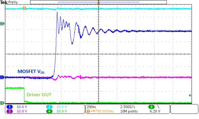
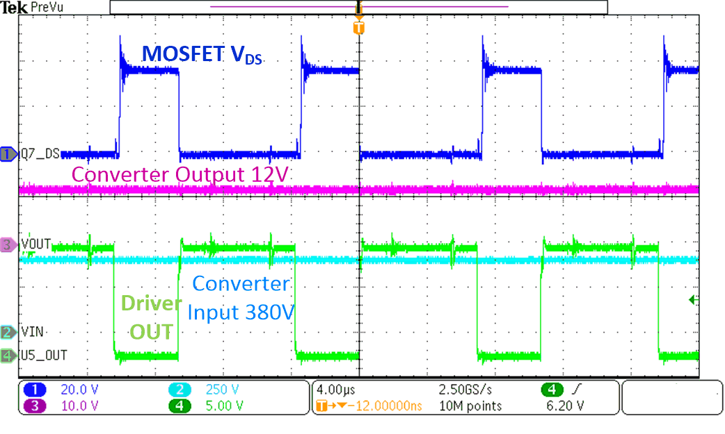
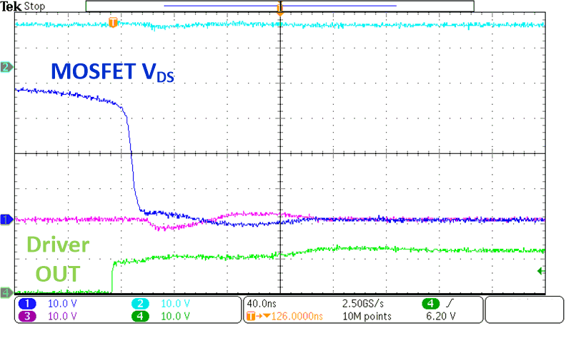
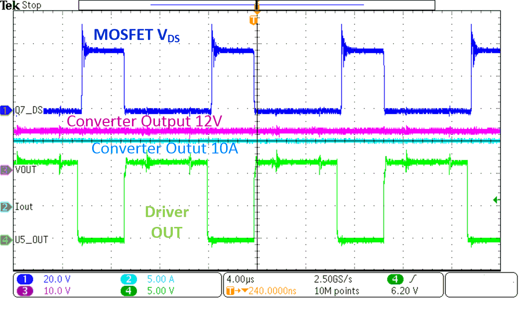
Many telecom and datacom isolated power modules employ synchronous rectification on the secondary side with center tap topology (as shown in Figure 8-2). The low-side driver UCC27614 can drive these synchronous rectifier MOSFETs as they are referenced to the output ground. These power modules are very power dense and the printed circuit board real estate is at a premium. These power modules may also have very high output current requirements and therefore either need very small Rds(on) MOSFETs or parallel multiple MOSFETs to achieve lower total Rds(on). In either case, the total get charge increases and therefore such applications need a gate driver with high drive current capability. UCC27614DSG fulfills all these requirements. The UCC27614DSG device is used in one such application of a 400-V to 12-V isolated DC-DC converter. Waveforms shown here are captured in this actual application power supply.
 Figure 8-5 Synchronous
Rectifier
MOSFET VDS
Rising
Edge
Using
UCC27614DSG
 Figure 8-7 Input
and
Output
Voltage
of
Converter
Using
UCC27614DSG
 Figure 8-6 Synchronous
Rectifier
MOSFET VDS
Falling
Edge
Using
UCC27614DSG
 Figure 8-8 Output
Voltage
and
Current
of a
Converter
Using
UCC27634DSG