SLUSD05B October 2017 – August 2018 UCC27710
PRODUCTION DATA.
- 1 Features
- 2 Applications
- 3 Description
- 4 Simplified Schematic
- 5 Revision History
- 6 Pin Configuration and Functions
- 7 Specifications
- 8 Detailed Description
-
9 Application and Implementation
- 9.1 Application Information
- 9.2
Typical Application
- 9.2.1 Design Requirements
- 9.2.2
Detailed Design Procedure
- 9.2.2.1 Selecting HI and LI Low Pass Filter Components (RHI, RLI, CHI, CLI)
- 9.2.2.2 Selecting Bootstrap Capacitor (CBOOT)
- 9.2.2.3 Selecting VDD Bypass/Holdup Capacitor (CVDD) and Rbias
- 9.2.2.4 Selecting Bootstrap Resistor (RBOOT)
- 9.2.2.5 Selecting Gate Resistor RON/ROFF
- 9.2.2.6 Selecting Bootstrap Diode
- 9.2.2.7 Estimate the UCC27710 Power Losses (PUCC27710)
- 9.2.2.8 Estimating Junction Temperature
- 9.2.2.9 Operation With IGBT's
- 9.2.3 Application Curves
- 10Power Supply Recommendations
- 11Layout
- 12Device and Documentation Support
- 13Mechanical, Packaging, and Orderable Information
Package Options
Mechanical Data (Package|Pins)
- D|8
Thermal pad, mechanical data (Package|Pins)
Orderable Information
8.3.6 Low Propagation Delays and Tightly Matched Outputs
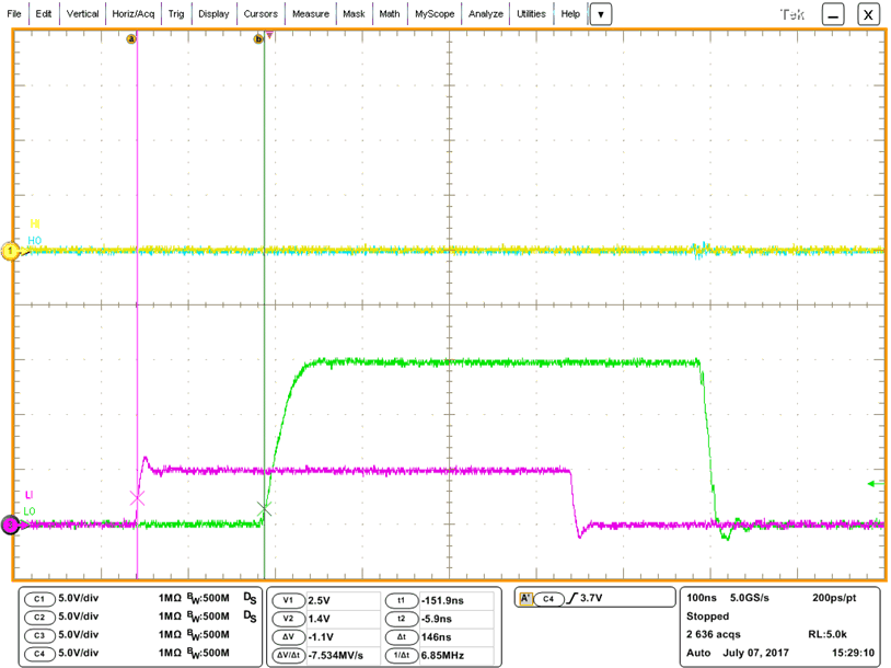
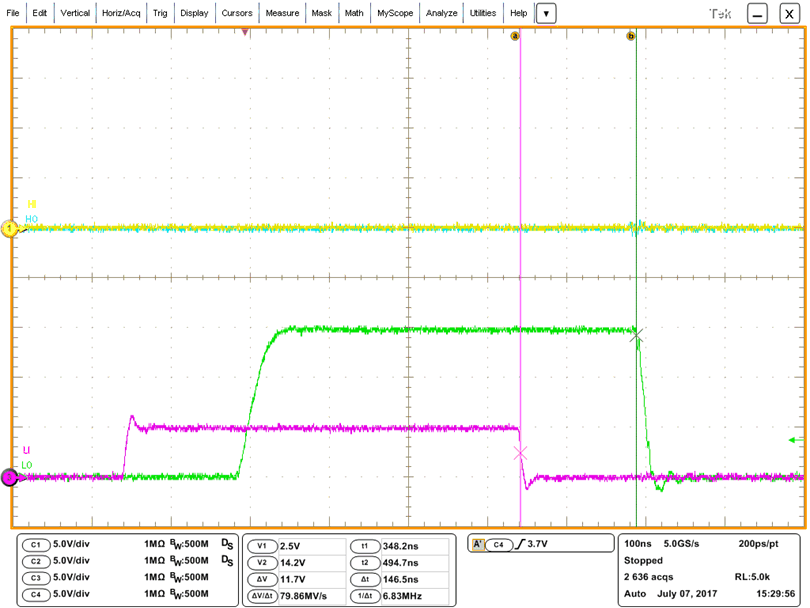
The UCC27710 features excellent, 140-ns (typical) propagation delay between input and output in high voltage 600-V driver, which goes to offer a low level of pulse width distortion.
 Figure 33. Turn-On Propagation Delay
  Figure 34. Turn-Off Propagation Delay